What is a Ćuk converter?
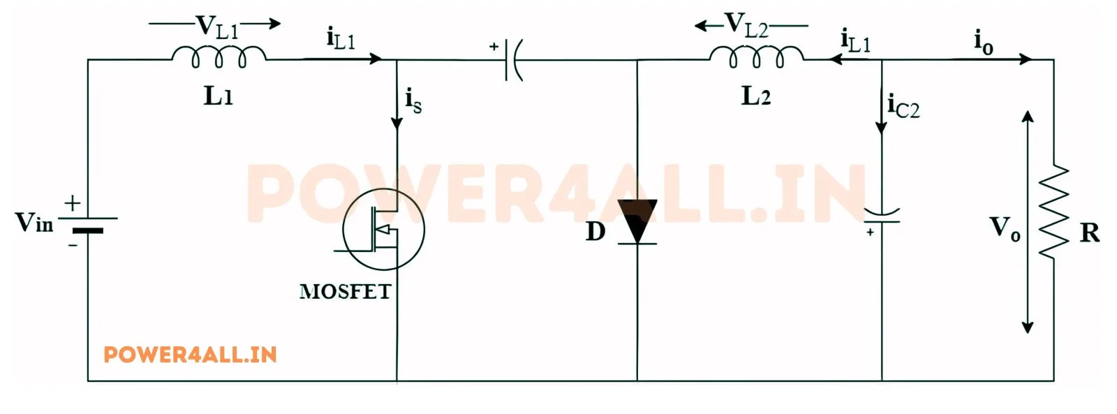
The Ćuk converter (named after Slobodan Ćuk) is a DC-DC converter that, like the buck-boost, produces an inverted output that can be higher or lower than the input — but it does so with far lower current ripple on both the source and the load. Its trick is to transfer energy through a series coupling capacitor C₁ rather than an inductor, with an input inductor L₁ and an output inductor L₂ smoothing the two port currents.
How it works — the two switching states
- Switch ON (0 → D·T): the MOSFET conducts; L₁ charges from Vin while the coupling capacitor C₁ discharges through L₂ into the output. The diode is off.
- Switch OFF (D·T → T): the diode conducts; L₁ recharges C₁ while L₂ maintains the output current. Volt-second balance on the two inductors sets the conversion ratio.
Key equations
This simulator numerically integrates the full 4th-order switching circuit (two inductors, two capacitors) with your device parasitics to steady state, then measures Vo, the coupling-cap voltage, the ripple and the losses from the resulting waveforms and compares them to the equations above.
Why the low ripple?
Because an inductor sits in series with both the input and the output, the source and load currents are continuous triangular waveforms rather than the pulsed currents of a basic buck-boost. This reduces conducted EMI at the input and ripple at the output — the Ćuk's main advantage. The cost is an extra inductor and capacitor, and a coupling capacitor C₁ that must handle a large RMS ripple current.
Ćuk vs SEPIC vs ZETA
| Converter | Polarity | Ideal Vo | Ripple |
|---|---|---|---|
| Ćuk | Inverting (−) | −D·Vin/(1−D) | Low in & out |
| SEPIC | Non-inverting (+) | D·Vin/(1−D) | Low input |
| ZETA | Non-inverting (+) | D·Vin/(1−D) | Low output |
See the SEPIC and ZETA simulators for the non-inverting relatives.
Applications
Low-noise negative-rail supplies, LED drivers, and any application where low input/output current ripple and a wide step-up/step-down range matter more than component count.
Frequently asked questions
What is the output voltage of a Ćuk converter?
In CCM the ideal output is Vo = −D·Vin/(1 − D) — negative, same magnitude as a buck-boost but with much lower ripple.
What is the coupling-capacitor voltage?
The average voltage across C₁ is Vin/(1 − D) = Vin + |Vo| — the simulator plots it live.
Why does the Ćuk have low ripple?
An inductor is in series with both the input and the output, so both port currents are smooth triangular waves rather than pulses.
What must the switch and diode withstand?
Both block the coupling-cap voltage Vin + |Vo| = Vin/(1 − D).