What is a SEPIC converter?
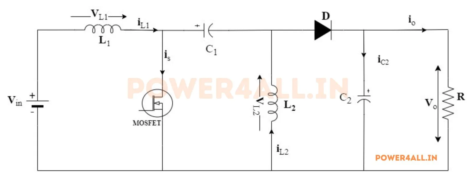
The SEPIC (Single-Ended Primary-Inductance Converter) is a DC-DC converter that produces a non-inverting (positive) output that can be higher or lower than the input. Like the Ćuk, it transfers energy through a series coupling capacitor C₁ and uses two inductors, but its output stays the same polarity as the input — a big practical advantage. It is a favourite for battery-powered supplies where the input voltage crosses the output during discharge.
How it works — the two switching states
- Switch ON (0 → D·T): the MOSFET conducts; L₁ charges from Vin and L₂ charges from the coupling capacitor C₁. The diode is off and the output capacitor supplies the load.
- Switch OFF (D·T → T): the diode conducts; both inductor currents flow into the output, and C₁ recharges from L₁. Volt-second balance sets the ratio.
Key equations
This simulator numerically integrates the full 4th-order switching circuit (two inductors, two capacitors) with your device parasitics to steady state, then measures Vo, the coupling-cap voltage, the ripple and the losses from the resulting waveforms and compares them to the equations above.
SEPIC vs buck-boost vs Ćuk
Compared with the inverting buck-boost, the SEPIC keeps the output positive and draws smooth input current (low EMI). Compared with the Ćuk, it is non-inverting but has a more pulsed output-capacitor current (so slightly higher output ripple). The switch and diode block Vin + Vo.
| Converter | Polarity | Ideal Vo | Ripple |
|---|---|---|---|
| Ćuk | Inverting (−) | −D·Vin/(1−D) | Low in & out |
| SEPIC | Non-inverting (+) | D·Vin/(1−D) | Low input |
| ZETA | Non-inverting (+) | D·Vin/(1−D) | Low output |
See the Ćuk and ZETA simulators for the related topologies.
Applications
Battery-to-rail supplies (e.g. 1–3 cell Li-ion to 3.3 V / 5 V), LED drivers, portable and automotive electronics, and any application needing a positive output that may be above or below the input while drawing smooth input current.
Frequently asked questions
What is the output voltage of a SEPIC converter?
In CCM the ideal output is Vo = D·Vin/(1 − D) — positive (non-inverting), step-down for D < 0.5 and step-up for D > 0.5.
What does SEPIC stand for?
Single-Ended Primary-Inductance Converter — a non-inverting step-up/step-down converter using two inductors and a coupling capacitor.
What is the coupling-capacitor voltage?
The average voltage across C₁ equals the input voltage, Vin. The simulator plots it live.
Why choose a SEPIC over a buck-boost?
A positive (non-inverting) output and low input current ripple, ideal for battery inputs where the source voltage crosses the output.