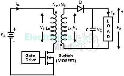
What is a flyback converter?
A flyback converter is the most widely used isolated DC-DC (SMPS) topology at low-to-medium power — every phone charger, standby supply and many auxiliary rails are flybacks. It looks like a buck-boost converter, but the single inductor is replaced by a transformer (coupled inductor), giving galvanic isolation between input and output and a free turns-ratio degree of freedom. A primary-side MOSFET stores energy in the transformer's magnetizing inductance while it is on; when it turns off, the stored energy "flies back" through the secondary winding and rectifier diode into the output capacitor.
How it works — the two switching states
Over each switching period T = 1/fsw the converter alternates between two states set by the duty cycle D (fraction of the period the switch is ON):
- Switch ON (0 → D·T): the primary is connected across Vs; the magnetizing current ramps up as
di_m/dt = Vs/Lm, storing energy. The secondary diode is reverse-biased, so the output capacitor alone supplies the load. - Switch OFF (D·T → T): the primary current is interrupted; the transformer voltage reverses, the secondary diode conducts, and the magnetizing energy is delivered to the output as the reflected current
i_sec = i_m/nramps down.
Key equations
This simulator does not plug numbers into these formulas — it numerically integrates the real flyback switching circuit (magnetizing inductance, reflected secondary current, output capacitor, with your device parasitics) to steady state, then measures Vo, the ripple and the losses and compares them to the equations above in the accuracy panel.
Continuous vs discontinuous conduction (CCM / DCM)
In CCM the magnetizing current never falls to zero and Vo = n·Vs·D/(1−D) holds. At light load or with a small magnetizing inductance the current hits zero each cycle — DCM — the diode stops conducting early, and the output voltage rises above the CCM value. The boundary is the critical inductance Lm(crit) = (1−D)²·R/(2·n²·fsw). Try the Light load → DCM preset and watch the magnetizing current touch zero.
Why the drain voltage spikes — leakage & snubbers (topic-specific)
Because primary and secondary are not perfectly coupled, some energy is stored in the leakage inductance Llk. At turn-off this current cannot transfer to the secondary instantly, so it rings against the MOSFET's output capacitance and produces a leakage voltage spike on top of the steady drain stress Vs + Vo/n. An RCD snubber or active clamp absorbs that energy and limits the peak. The simulator's stress meter shows the peak drain voltage live, and the RCD-clamp toggle demonstrates how the spike is tamed — a core part of real flyback design.
Advanced options in this simulator
- Turns ratio & duty: sweep n = Ns/Np and D to step up or step down while keeping isolation.
- Magnetizing & leakage inductance: set the CCM/DCM boundary and the turn-off drain spike independently.
- Drain-stress meter: live peak drain voltage = Vs + Vo/n + leakage spike, with an RCD-clamp option.
- Device model: MOSFET Rds(on), diode Vf, winding DCR and capacitor ESR; the accuracy check stays locked to the ideal Vo.
- Ripple spectrum: a real FFT of the output voltage or the diode current, with harmonics at multiples of fsw.
- Export & capture: download the full waveform data as CSV, a text report, or a PNG screenshot of the scope.
The six isolated DC-DC converters
| Converter | Switches | Ideal Vo | Filter |
|---|---|---|---|
| Flyback | 1 | n·Vs·D/(1−D) | Output cap only |
| Forward | 1 | n·Vs·D | LC filter |
| Push-Pull | 2 (center-tap) | 2·n·Vs·D | LC filter |
| Half-Bridge | 2 + split caps | n·Vs·D | LC filter |
| Full-Bridge | 4 | 2·n·Vs·D | LC filter |
| Phase-Shifted FB | 4 (ZVS) | 2·n·Vs·Deff | LC filter |
Explore the others: Forward, Push-Pull, Half-Bridge, Full-Bridge and Phase-Shifted Full-Bridge simulators. For the full theory see the Flyback converter tutorial.
Applications
Phone and laptop chargers, standby/auxiliary supplies, offline AC-DC adapters, bias supplies for larger converters, LED drivers, isolated gate-drive supplies and low-power industrial SMPS. The flyback dominates isolated power below ~100 W.
Frequently asked questions
What is the output voltage of a flyback converter?
In CCM the ideal output is Vo = n·Vs·D/(1−D), where n = Ns/Np is the turns ratio. The transformer scales the reflected voltage, so a flyback can step up or down while staying isolated.
How does a flyback provide isolation?
It uses a transformer (coupled inductor) instead of a plain inductor. Energy is stored on the primary during the on-time and delivered through a separate secondary winding during the off-time, so input and output share no electrical connection.
What causes discontinuous conduction (DCM)?
Light load or a small magnetizing inductance lets the magnetizing current reach zero each cycle. Below Lm(crit) = (1−D)²·R/(2·n²·fsw) the flyback enters DCM and the output rises above the CCM value.
Why does the MOSFET see a voltage spike?
The drain blocks Vs + Vo/n plus a leakage-inductance ringing spike at turn-off. An RCD snubber or active clamp limits it — toggle the clamp and watch the drain-stress meter.
How do I pick the turns ratio?
n = Ns/Np sets the output voltage and trades duty cycle against drain-voltage stress. Designers choose n so the duty sits near 0.35–0.5 at nominal input while keeping the reflected voltage (and drain stress) within the MOSFET rating.