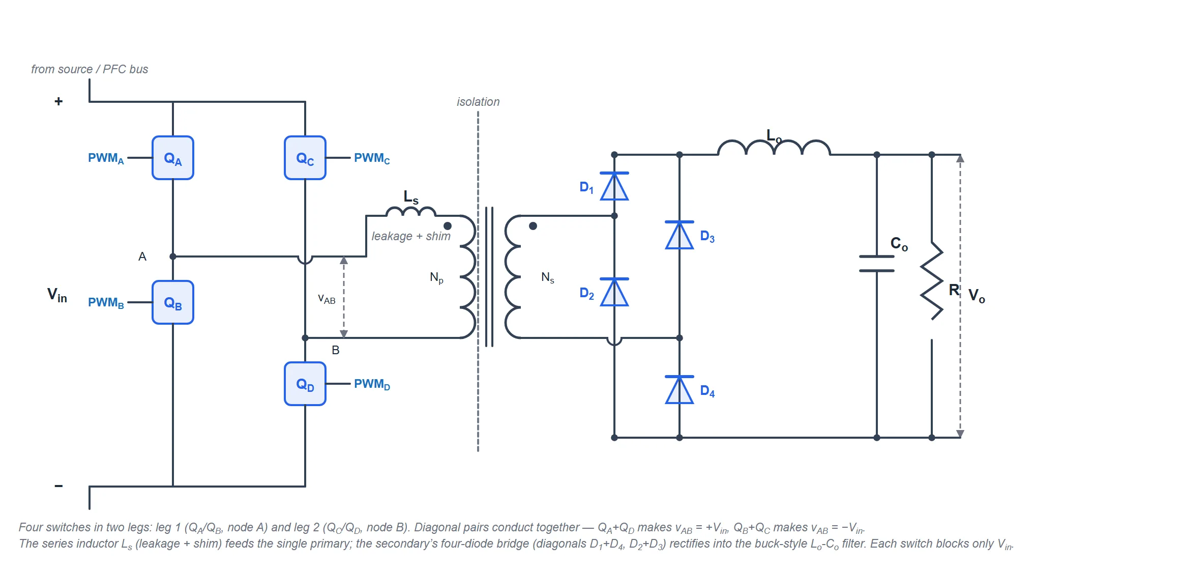
What is a full-bridge converter?
A full-bridge converter (also called an H-bridge DC-DC converter) uses four switches to apply the full input voltage ±Vs across the transformer primary. Diagonal pair Q1-Q4 drives +Vs; diagonal pair Q2-Q3 drives −Vs. The full-wave-rectified secondary feeds a buck-like LC filter. Because it applies twice the primary voltage of a half-bridge at the same switch stress (Vs), the full-bridge delivers the highest power of the isolated topologies — the standard choice above roughly 500 W.
How it works
- Q1 + Q4 ON (0 → D·T): the primary sees +Vs; the secondary applies
n·Vsto the LC filter — first power pulse. - Dead-time: all switches off; the rectifier freewheels (node = 0).
- Q2 + Q3 ON (T/2 → T/2+D·T): the primary sees −Vs; the full-wave rectifier again applies
n·Vs— second power pulse. - Dead-time to the end of the period.
Key equations
This simulator numerically integrates the real full-bridge circuit — the ±Vs diagonal drive, the DC-blocking capacitor, the magnetizing current and the output LC — to steady state, then compares the measured Vo and ripple to the equations above in the accuracy panel.
Diagonal gating & the DC-blocking capacitor (topic-specific)
The four switches operate as two diagonal pairs. Getting the gating right — and inserting a dead-time so the two switches in a leg never conduct together — is central to a reliable full-bridge; overlap causes a destructive shoot-through straight across the bus. Like the push-pull, a full-bridge can suffer flux imbalance if the diagonals apply unequal volt-seconds, so a small DC-blocking capacitor in series with the primary is used to block DC current and keep the flux centred. This simulator shows the live diagonal-gating map, the DC-block cap voltage (which self-centres near zero) and the dead-time margin.
Why the full-bridge handles the most power
The full ±Vs primary drive gives twice the output of a half-bridge for the same Vs switch stress, and the four switches share the current — so for a given device rating the full-bridge processes the most power. The cost is four switches and four gate drives instead of two. It dominates high-power isolated conversion: EV chargers, welding supplies, telecom rectifiers and industrial DC-DC.
Advanced options in this simulator
- Diagonal-gating map: watch which of the four switches conduct (Q1-Q4 / Q2-Q3) each half-cycle.
- DC-block capacitor: see it self-centre near zero and keep the flux balanced.
- Dead-time / shoot-through guard: live margin as duty approaches 0.5.
- Vs switch-stress meter: the best switch-utilisation of the isolated topologies.
- Device model: MOSFET Rds(on), diode Vf, inductor DCR and capacitor ESR; the accuracy check stays locked to the ideal Vo.
- Ripple spectrum & export: FFT at twice fsw, plus CSV/report/PNG.
The six isolated DC-DC converters
| Converter | Switches | Ideal Vo | Switch stress |
|---|---|---|---|
| Flyback | 1 | n·Vs·D/(1−D) | Vs + Vo/n |
| Forward | 1 | n·Vs·D | Vs·(1+Np/Nr) |
| Push-Pull | 2 (center-tap) | 2·n·Vs·D | 2·Vs |
| Half-Bridge | 2 + split caps | n·Vs·D | Vs |
| Full-Bridge | 4 | 2·n·Vs·D | Vs |
| Phase-Shifted FB | 4 (ZVS) | 2·n·Vs·Deff | Vs |
Explore the others: Flyback, Forward, Push-Pull, Half-Bridge and Phase-Shifted Full-Bridge simulators. For the full theory see the Full-Bridge converter tutorial.
Applications
High-power isolated DC-DC: EV and battery chargers, welding and plating supplies, telecom and server rectifiers, solar and industrial power, and the front-end for phase-shifted ZVS full-bridge designs.
Frequently asked questions
What is the output voltage of a full-bridge converter?
In CCM the ideal output is Vo = 2·n·Vs·D, where D is the duty of each diagonal pair (≤0.5). The ±Vs primary drive doubles the output of a half-bridge.
How do the four switches operate?
As two diagonal pairs: Q1-Q4 for +Vs, then Q2-Q3 for −Vs, with a dead-time between so a leg never shorts.
Why a DC-blocking capacitor?
It blocks DC primary current from unequal switch timing, preventing flux-staircase saturation. Its voltage self-centres near zero.
Full-bridge vs half-bridge?
The full-bridge applies ±Vs with four switches (Vo = 2·n·Vs·D), double the half-bridge's ±Vs/2 output — for the same Vs switch stress and more power.
What is the switch voltage stress?
Only Vs — the same as a half-bridge and half a push-pull — giving the best switch utilisation of the isolated topologies.