Full-Bridge Converter
The four-switch isolated buck — two switch legs drive the transformer with the full ±Vin while each switch still blocks only Vin. Full drive voltage at half-bridge stress: that is why it owns the top of the power range, from a few hundred watts to many kilowatts.
- Introduction — finishing what the half-bridge started
- What is a Full-Bridge Converter?
- Block Diagram
- Circuit Diagram & Construction
- Principle of Operation
- Modes of Operation
- Waveforms Explained in Detail
- Series Inductor Ls & Duty-Cycle Loss
- Phase-Shift Control & ZVS
- Output Rectifier Options
- Key Formulas
- Voltage Gain & Turns Ratio
- Worked Example — and the family showdown
- Advantages & Disadvantages
- Applications
- Frequently Asked Questions – FAQs
- Related Topics
Introduction — finishing what the half-bridge started
The half-bridge converter made one great trade: by driving the transformer from a capacitor mid-rail at Vin/2, it cut the switch stress to just Vin. But that trade has a hidden bill — at half the voltage, the primary must carry twice the current for the same power. Push a half-bridge past a few hundred watts and its switches and windings start cooking on conduction loss.
The full-bridge converter collects the best of both worlds. It replaces the half-bridge’s two divider capacitors with a second switch leg, so the transformer primary hangs between two switching nodes. Turning on a diagonal pair of switches applies the full +Vin across the primary; the opposite diagonal applies −Vin. The primary gets the full drive voltage — so the current halves back down — yet each switch still never sees more than Vin. Full voltage and low stress. The price: four switches, two of them floating high-side drives.
This page builds the full-bridge from that idea: the two-leg power stage, what each diagonal pair does, the waveforms on a scope, the series inductor Ls and the duty-cycle loss it causes, the phase-shift drive that turns this topology into the soft-switched workhorse of modern multi-kilowatt supplies, the formulas, and a worked example that lines the whole isolated-buck family up side by side.
What is a Full-Bridge Converter?
A full-bridge converter (or H-bridge converter) is an isolated switch-mode DC-DC converter that behaves like a buck converter fed through a transformer driven at the full input voltage in both directions. It is built from these parts:
- Four switches (MOSFETs) in two legs. Leg 1 is QA (high-side) over QB (low-side), meeting at node A; leg 2 is QC over QD, meeting at node B. Both legs sit directly across Vin.
- A single-primary transformer between nodes A and B. The bridge voltage vAB drives it at ±Vin — both magnetic directions, so no reset winding is needed.
- A series inductor Ls in the primary loop — partly the transformer’s own leakage, often topped up with a small discrete inductor. It looks like a parasitic, but it is a design element: it sets the duty-cycle loss and (in phase-shifted designs) provides the energy for zero-voltage switching.
- A four-diode bridge rectifier on the single secondary winding. One diagonal diode pair (D1+D4) conducts when the secondary is positive, the other (D2+D3) when it is negative.
- An output L-C filter (Lo, Co) that smooths the rectified pulses into clean DC, exactly as in a buck.
The heart of it is the diagonal drive. QA+QD on together connects node A to Vin and node B to ground: vAB = +Vin. Half a period later QB+QC reverse it: vAB = −Vin. The transformer sees a symmetric AC square wave at the full rail — twice the half-bridge’s swing — and whichever switches are off are clamped by their own leg to exactly Vin.
Block Diagram
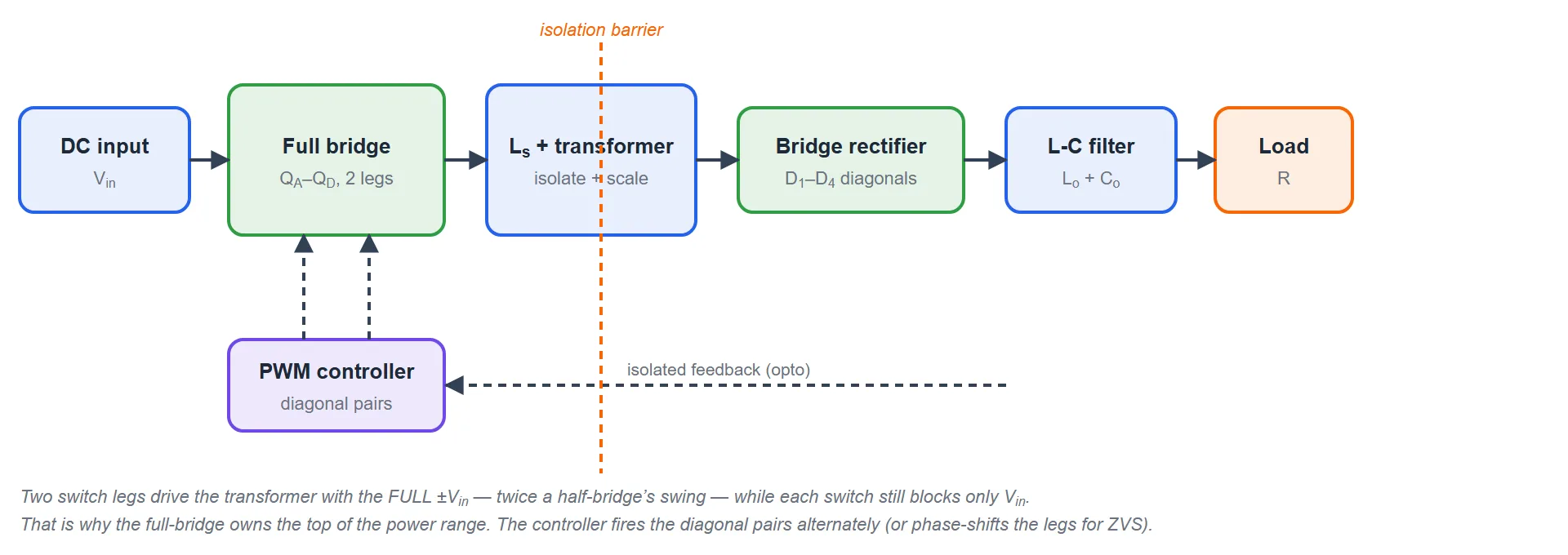
Read it left to right as a power path: the DC input is chopped by the four-switch bridge, driven through the series inductor and transformer, rectified by the four-diode bridge, smoothed by the L-C filter, and delivered to the load. Two things mark it as a full-bridge. First, there is no capacitor divider — the second switch leg replaces it, so the transformer swings the full ±Vin. Second, the controller fires diagonal pairs (or, in the phase-shifted variant, slides one leg’s phase against the other). As always, feedback crosses the isolation barrier through an opto-coupler.
Circuit Diagram & Construction
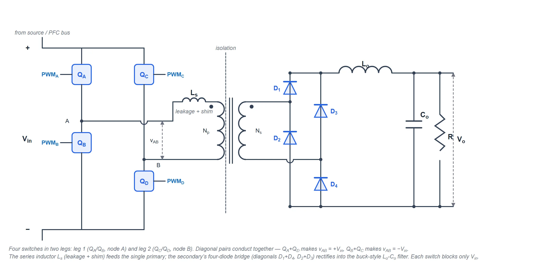
This is the power stage, drawn and labelled in our own schematic style. Tracing it across:
| Switch legs QA/QB and QC/QD | Two half-bridge legs directly across Vin, making switching nodes A and B. Within each leg the two switches are complementary (never both on); across the bridge, diagonal pairs conduct together. QA and QC need floating high-side gate drives; each switch blocks only Vin. |
|---|---|
| Series inductor Ls | The transformer’s leakage inductance plus, usually, a small discrete “shim” inductor. It slows the primary-current polarity reversal (causing duty-cycle loss, below) and stores the energy that makes zero-voltage switching possible in phase-shifted designs. |
| Transformer (single primary Np, single secondary Ns) | Driven between nodes A and B at ±Vin. Symmetric AC drive — the core swings both ways, no reset winding, no air gap. Simple two-winding construction: the best copper utilisation in the whole isolated family. |
| Bridge rectifier D1–D4 | Four diodes on the single secondary. Diagonal pair D1+D4 conducts when the secondary voltage is positive, D2+D3 when negative; all four share the current during the dead time. Each diode blocks only n·Vin (= Vo/Deff). |
| Output filter Lo, Co | A buck-type L-C filter. Fed twice per period, so the inductor current ripples at twice the switching frequency. |
Principle of Operation
The four gates come from one controller. In the classic hard-switched drive, the two diagonal pairs are fired alternately, each for a fraction D of the full period (D < 0.5), 180° apart. Over one period there are four intervals: pair 1 on, dead time, pair 2 on, dead time:
- When QA+QD are on, node A is at Vin and node B at ground, so vAB = +Vin. The secondary produces +n·Vin, diagonal D1+D4 conducts, and energy passes straight through to the Lo-Co filter. The output inductor charges.
- When QB+QC are on, the bridge reverses: vAB = −Vin. The secondary produces −n·Vin, the other diagonal D2+D3 conducts, and the filter is fed again. The core magnetises the opposite way — resetting itself.
- In the dead times (all four off), the transformer is quiet but the output inductor keeps its current flowing: all four rectifier diodes conduct, the secondary is effectively shorted, and the inductor freewheels.
So the load is fed twice per switching period and the transformer sees a symmetric AC square wave at the full rail. The output voltage follows from volt-second balance on the output inductor, exactly as in a buck — the transformer just scales the pulse height by n.
Modes of Operation
A full-bridge has two driven states — one per diagonal pair — separated by dead times in which the output inductor freewheels. Trace each state on the power circuit of Figure 2 above; the current path is described in words below.
Mode 1 — QA + QD ON (vAB = +Vin)
- Current flows from the + rail through QA to node A, through Ls and the primary to node B, and down through QD to the − rail. The full Vin sits across the Ls-primary loop, and the core magnetises in the “positive” direction.
- On the secondary, +n·Vin forward-biases the diagonal D1 (secondary top → + rail) and D4 (− rail → secondary bottom). The inductor Lo sees (n·Vin − Vo) and its current ramps up, delivering power to the load.
- QB and QC are off; each is clamped by its own conducting leg partner to exactly Vin. D2 and D3 block n·Vin.
Mode 2 — QB + QC ON (vAB = −Vin)
- Half a period later the opposite diagonal conducts: current flows through QC to node B, backwards through the primary and Ls to node A, and down through QB. The primary sees the full Vin in the opposite polarity, so the core magnetises the other way — this is what resets the flux without any reset winding.
- The secondary now produces −n·Vin, forward-biasing the other diagonal D3+D2, so the output inductor charges exactly as in Mode 1. From the output’s point of view the two modes are identical.
- QA and QD are now off, each blocking Vin.
Dead time — all four off (freewheel)
- Between the driven states, all four switches are off. The transformer delivers no power, but Lo’s current cannot stop.
- With no secondary polarity enforced, all four rectifier diodes conduct together, splitting the inductor current between the two diagonals. The secondary is effectively short-circuited, so the inductor sees −Vo and its current ramps gently down until the next pair fires.
- Because the shorted secondary also clamps the primary voltage to zero, the magnetising current simply circulates (reflected into the secondary loop) and the switching nodes settle toward Vin/2. This freewheel is the same job a buck’s freewheel diode does.
Waveforms Explained in Detail
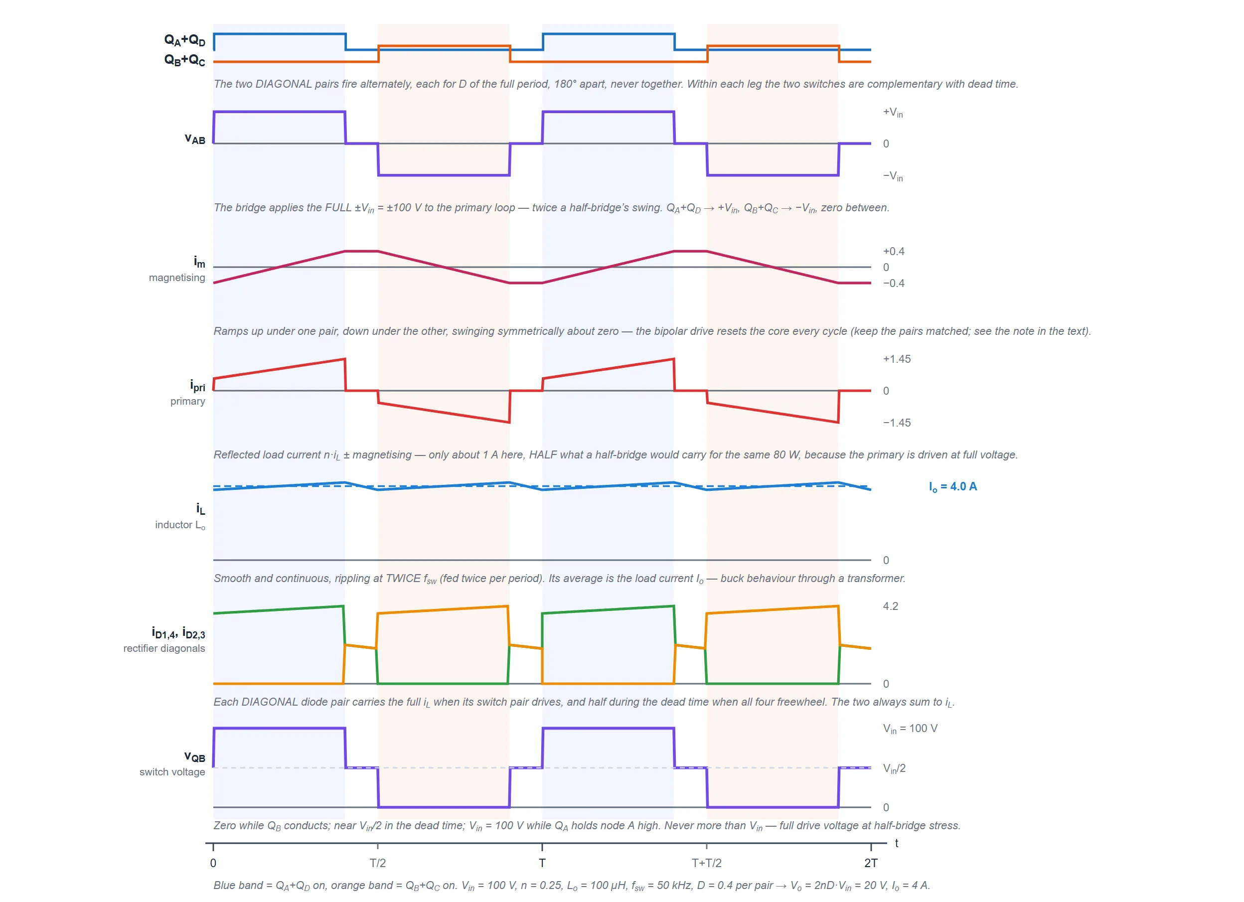
Read the traces together and the whole converter is visible in one picture:
- Gates. The two diagonal pairs fire alternately, each for D of the full period, 180° apart, never overlapping. Within each leg, the two switches are complementary with a dead-time guard.
- Bridge voltage vAB. A symmetric AC square wave at the full ±Vin (±100 V here) — twice the half-bridge’s swing. This is the whole point of the second leg.
- Magnetising current im. Ramps up under one pair, down under the other, swinging symmetrically about zero — the core resets itself every period.
- Primary current ipri. The reflected load current n·iL plus magnetising — only about ±1 A here. A half-bridge doing the same 80 W carries about ±2 A. Halving the primary current (and its conduction loss) is the full-bridge’s scaling advantage.
- Inductor current iL. A smooth triangle rippling at twice the switching frequency, because the filter is topped up twice per period. Its average is the load current.
- Rectifier diagonals. Each diagonal pair carries the full inductor current while its switch pair drives, and half during the dead-time freewheel. At every instant they sum to iL — the output never breaks.
- Switch voltage vQB. Zero while QB conducts, about Vin/2 in the dead time, and Vin = 100 V while QA holds node A high. Full drive voltage, half-bridge stress.
Series Inductor Ls & Duty-Cycle Loss
Look back at the circuit: between the bridge and the transformer sits the series inductor Ls — the transformer’s leakage plus, in most real designs, a deliberate extra few microhenries. It creates the full-bridge’s most distinctive non-ideality, and understanding it is what separates a paper design from a working one.
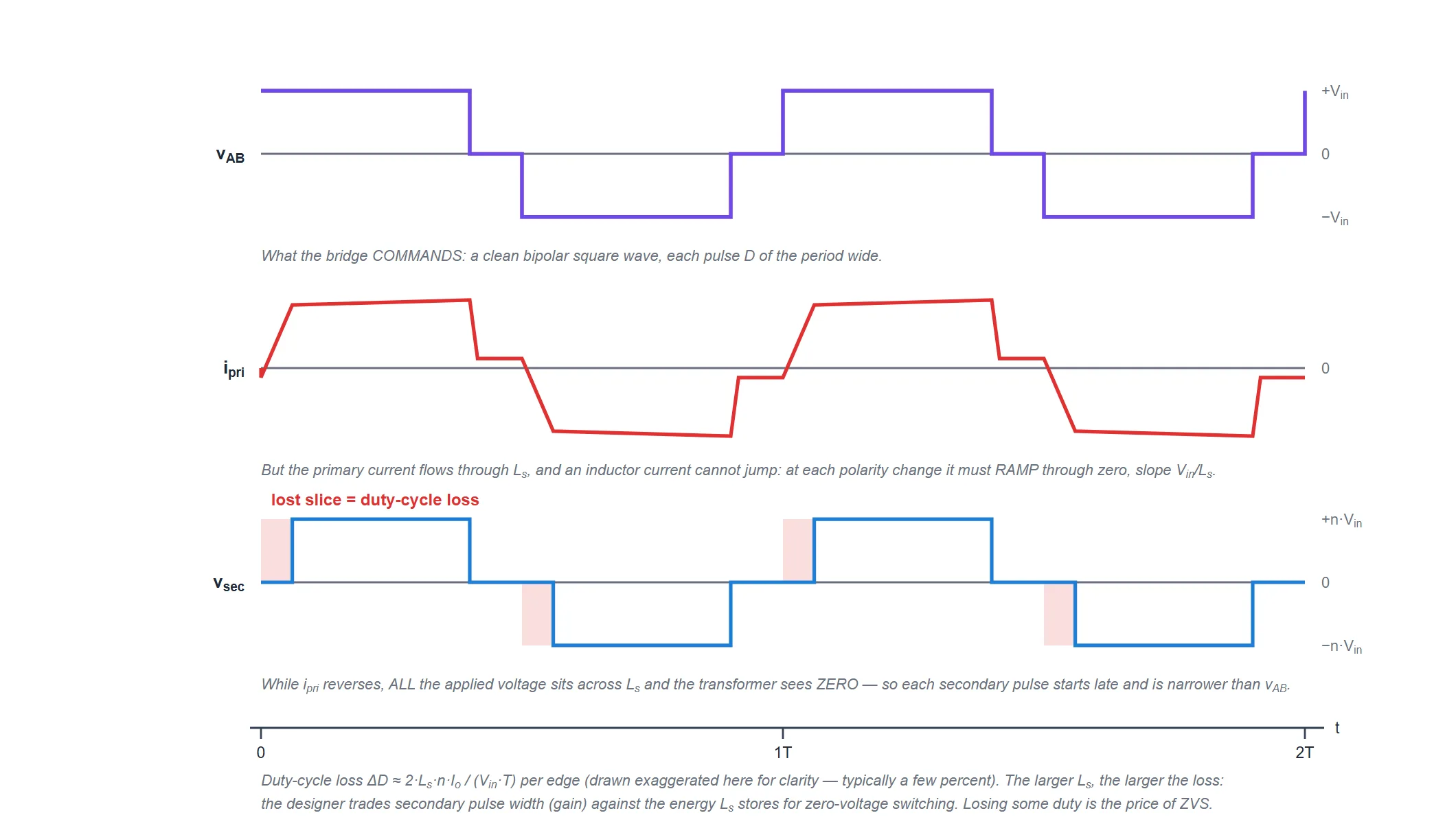
Here is the mechanism, one step at a time. When the bridge flips vAB from one polarity to the other, the primary current must also reverse — but it flows through Ls, and an inductor’s current cannot jump. So for a short interval the entire applied Vin sits across Ls, ramping its current through zero at a slope of Vin/Ls, while the transformer itself sees zero volts. During that interval the secondary delivers nothing. The result: each secondary pulse (vsec) starts late and is narrower than the vAB pulse that commanded it. The difference is called duty-cycle loss, and the effective duty that actually reaches the output is Deff < D. The larger Ls (or the heavier the load current it must reverse), the larger the loss.
Phase-Shift Control & ZVS — the modern way to drive it
Everything above used the classic drive: fire the diagonal pairs together, vary their width. Modern high-power designs almost always use a smarter scheme — the phase-shifted full-bridge (PSFB):
- Each leg runs at a fixed ~50 % duty (complementary top/bottom switches with dead time), so every node swings rail-to-rail every period, always.
- The control variable is the phase between leg 1 and leg 2. When the legs are in phase, the two ends of the primary move together and vAB = 0 — no output. As leg 2’s timing slides against leg 1’s, an overlap opens up in which one node is high while the other is low, and vAB carries ±Vin for that overlap. The phase shift is the effective duty cycle.
- Zero-voltage switching (ZVS) comes free. In the dead time before each switch turns on, the current stored in Ls keeps flowing and discharges that switch’s output capacitance (Coss), pulling its drain-source voltage to zero — the current briefly flows backwards through the switch position — before the gate rises. The switch then turns on with no voltage across it, so the turn-on switching loss essentially vanishes.
This is why the phase-shifted full-bridge dominates the multi-kilowatt world: it keeps the full-bridge’s low stresses and full drive voltage, and removes most of the switching loss that would otherwise cap the switching frequency. A representative modern design point: a 54 V, 3 kW server/telecom rectifier stage switching at 140 kHz. The catch is light load: with little current in Ls, there is not enough energy to discharge Coss, ZVS is lost, and the controller must manage it (burst modes, adaptive dead time). The phase-shifted full-bridge has its own detailed page — leading vs lagging leg, the resonant tank and the full ZVS story; here it is enough to see that it is this same power stage, driven by phase instead of pulse width.
Output Rectifier Options
Figure 2 shows the four-diode bridge, but the full-bridge primary works with any full-wave secondary. The three standard choices, and when each wins:
| Rectifier | Diodes / FETs | Device voltage stress | Best suited for |
|---|---|---|---|
| Full-bridge (Fig 2) | 4 | Vo/Deff = n·Vin (lowest) | Higher output voltages — two devices conduct in series, but each blocks only half what a centre-tap’s would. |
| Centre-tapped | 2 | 2·Vo/Deff = 2·n·Vin | Low output voltage / high current — only ONE diode drop in the path, but each device blocks double and the winding needs a centre tap. |
| Current doubler | 2 (+ two output inductors) | Vo/Deff | Very high current outputs — each inductor carries half the load current and the secondary is a simple single winding; the trade is Deff capped at 50 %. |
In high-current designs all of these are usually built with synchronous rectifiers — MOSFETs in place of diodes, gated to conduct when their diode would — recovering the diode drop as efficiency. Our worked example keeps ideal diodes for clarity.
Key Formulas
All from volt-second balance on the output inductor, with n = Ns/Np and D the duty of each diagonal pair (D ≤ 0.5). Deff = 2D is the fraction of the period the secondary carries voltage.
Output voltage (CCM). The filter is fed n·Vin for 2D of the period and 0 for the rest:
(n·Vin − Vo)·2D·T = Vo·(1 − 2D)·T → Vo = 2 · n · D · Vin (= n · Deff · Vin)Twice the half-bridge’s Vo = nD·Vin at the same turns ratio — the full ±Vin drive restores the factor of 2.
Duty ratio for a target output. Rearranging:
D = Vo / (2 · n · Vin) (must stay < 0.5)Inductor-current ripple and average. Standard buck filter, ripple repeating every half period:
ΔiL = (n·Vin − Vo)·D·T / Lo | IL,avg = IoDevice stress. Each off switch is clamped by its own leg; each bridge-rectifier diode sees the secondary pulse:
Switch: VQ,off = Vin | Diode: VD,rev = n · Vin = Vo/DeffCurrents. The primary carries the reflected load current at full drive voltage:
Ipri ≈ n · Io | Iin,avg = 2 · D · n · Io = Po / VinDuty-cycle loss. The slice of each pulse spent reversing Ls’s current:
ΔD ≈ 2 · Ls · n · Io / (Vin · T) per edge → use Deff = 2D − ΔDtotal in the gain formula(Switch and diode drops, winding resistance and losses are neglected; a hard-switched full-bridge is typically 90–94 % efficient, and a well-designed phase-shifted version with synchronous rectifiers can exceed 96 %.)
Voltage Gain & Turns Ratio
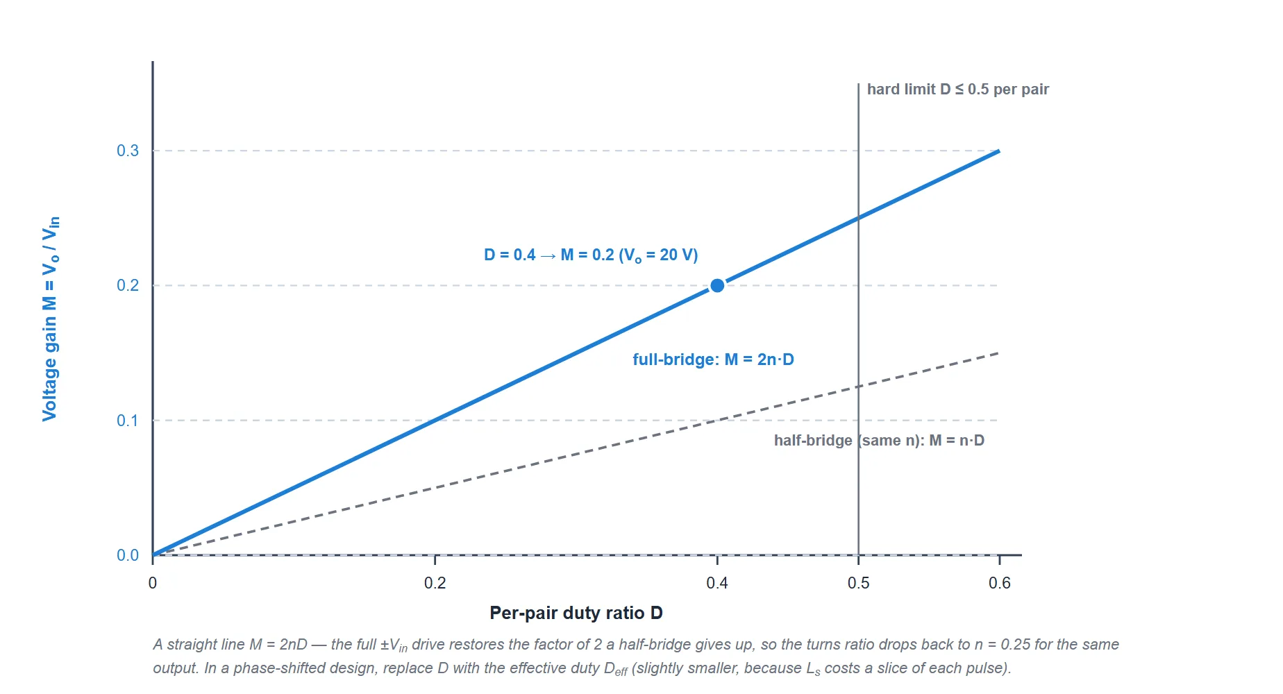
The full-bridge’s gain is a straight line, M = 2n·D — easy to control, and twice a half-bridge’s at the same turns ratio, because the primary is driven at Vin instead of Vin/2. Like all its buck-derived relatives it is fundamentally a step-down through a transformer. Key points:
- The turns ratio does the coarse scaling. Here n = 0.25 puts the 100 V → 20 V operating point at a comfortable D = 0.4 — the same n a push-pull would use, half what a half-bridge needs.
- The duty is hard-capped at 0.5 per pair by the leg dead times, so the maximum output is n·Vin. Phase-shifted designs replace D with Deff, slightly smaller because of duty-cycle loss.
- Continuous inductor current keeps it linear. Very light load can push Lo into discontinuous conduction, where the output rises above 2nD·Vin and becomes load-dependent; the inductor is sized to stay continuous over the working range.
Worked Example — and the family showdown
One consistent design, used by every figure above. Follow the numbers and the formulas check out.
| Given | Vin = 100 V, Ns:Np = 1:4 (n = 0.25), D = 0.4 per pair, f = 50 kHz (T = 20 µs), Lo = 100 µH, Lm = 1 mH |
|---|---|
| Primary swing ±Vin | ±100 V (double a half-bridge’s ±50 V) |
| Output voltage Vo = 2·n·D·Vin | 2 × 0.25 × 0.4 × 100 = 20 V |
| Load (for Io = 4 A) R = Vo/Io, Po = VoIo | R = 5 Ω, Po = 80 W |
| Secondary pulse voltage n·Vin | 0.25 × 100 = 25 V (applied Deff = 2D = 0.8 of the period) |
| Inductor ripple ΔiL = (n·Vin−Vo)·D·T/Lo | (25−20) × 0.4 × 20µ/100µ = 0.4 A at 2f (Imax 4.2, Imin 3.8 → CCM) |
| Magnetising swing Δim = Vin·D·T/Lm | 100 × 0.4 × 20µ/1m = 0.8 A bipolar (±0.4 A about zero) |
| Switch voltage stress Vin | 100 V (same as half-bridge; a push-pull would be 200 V) |
| Rectifier diode reverse n·Vin = Vo/Deff | 25 V (= 20/0.8 ✓; a centre-tap secondary would double this to 50 V) |
| Primary current (driving) ≈ n·Io | ≈ 1 A (a half-bridge doing the same job carries ≈ 2 A) |
| Input current (avg) 2·D·n·Io | 2 × 0.4 × 0.25 × 4 = 0.8 A → Pin = 100 × 0.8 = 80 W = Po ✓ |
The last row is the lossless sanity check: 80 W in, 80 W out. And now the payoff of using the same 100 V → 20 V / 4 A job on all three double-ended pages — the whole trade-off landscape in one table:
| Same job: 100 V → 20 V, 4 A | Push-pull | Half-bridge | Full-bridge |
|---|---|---|---|
| Primary drive | ±Vin = ±100 V | ±Vin/2 = ±50 V | ±Vin = ±100 V |
| Turns ratio needed | 0.25 (per half) | 0.5 | 0.25 |
| Switch voltage stress | 200 V (2·Vin) | 100 V | 100 V |
| Primary current (approx.) | ≈ 1 A | ≈ 2 A | ≈ 1 A |
| Switches / floating drives | 2 / none | 2 / one | 4 / two |
| Sweet spot | Low-voltage input, 150 W–1 kW | Off-line, 100–500 W | Off-line, 500 W and up |
Each column pays for its advantage somewhere else: the push-pull’s simple ground drive costs double switch stress; the half-bridge’s low stress costs double current; the full-bridge pays in switch count and gate-drive complexity to get full voltage and low stress — which is exactly the trade you want once the power is high enough to make silicon cheaper than heat.
Advantages & Disadvantages
Advantages
- Full drive voltage at low stress. The primary sees ±Vin yet each switch blocks only Vin — the best voltage economics in the isolated family, ideal off a rectified line or PFC bus.
- Half the primary current of a half-bridge at the same power — lower conduction loss, so it scales to kilowatts.
- Best transformer utilisation. A simple two-winding transformer, driven both ways (no reset winding, no centre-tap copper waste), fed twice per period into a small filter.
- ZVS-capable. Driven phase-shifted, the same power stage soft-switches using Ls’s energy — high frequency and high efficiency together.
- Isolation, multiple outputs, and a clean low-ripple output, like any transformer-isolated converter.
Disadvantages
- Four switches and two floating gate drives — the highest parts count and drive complexity in the family; overkill below a few hundred watts.
- Duty-cycle loss from Ls shaves the effective duty, forcing a slightly larger turns ratio; leakage energy must be managed.
- No built-in flux balancing in the basic circuit (no series blocking capacitor) — volt-second imbalance can walk the core, so practical designs rely on current-mode control or add a blocking cap.
- Shoot-through risk per leg demands reliable dead-time generation for two legs, not one.
- ZVS is load-dependent in phase-shifted designs — it fades at light load and the controller must compensate.
Applications
- High-power off-line supplies, ~500 W to tens of kW — the topology of choice once a half-bridge’s doubled current stops making sense.
- Server and telecom rectifiers — e.g. a 54 V / 3 kW phase-shifted stage at 140 kHz behind a PFC front end.
- EV on-board chargers and DC fast-charging modules, where the PSFB (and its resonant cousins) dominate.
- Industrial equipment: welding supplies, plating, induction heating, high-power battery chargers.
- Renewable-energy converters — isolated DC-DC stages in solar and storage systems.
- The front half of many inverters, boosting and isolating a battery bus before the DC-AC stage.
The rule of thumb completes the family: flyback/forward below ~100 W, push-pull for low-voltage inputs to ~1 kW, half-bridge off-line to ~500 W, and full-bridge for everything above — hard-switched when simple, phase-shifted with ZVS when efficiency and frequency matter.
Frequently Asked Questions – FAQs
Related Topics
- Phase-Shifted Full-Bridge — the soft-switched (ZVS) version
- Half-Bridge Converter — the split-rail little brother
- Push-Pull Converter — the dual-switch isolated buck
- Forward Converter — the single-switch isolated buck
- Flyback Converter — the low-power isolated buck-boost
- Buck Converter (Step-Down) — the non-isolated parent
- DC-DC Converters — Overview
- MOSFET — the usual bridge switch
- All Power Electronic Converters