Forward Converter
The isolated buck — a transformer, one switch, and an L-C output filter. Energy passes straight through to the load while the switch is on, an inductor keeps it flowing while the switch is off, and a reset winding empties the core each cycle.
- Introduction — isolation that passes energy through
- What is a Forward Converter?
- Block Diagram
- Circuit Diagram & Construction
- Principle of Operation
- Modes of Operation
- The Reset Winding & the D ≤ 0.5 Limit
- Waveforms Explained in Detail
- Key Formulas
- Voltage Gain & Turns Ratio
- Worked Example
- Forward vs Flyback
- Advantages & Disadvantages
- Applications
- Frequently Asked Questions – FAQs
- Related Topics
Introduction — isolation that passes energy through
The flyback converter gives isolation by storing energy in its transformer and releasing it later. The forward converter does the opposite: it uses the transformer the way a transformer is normally used — energy is passed straight through from primary to secondary at the same instant, while the switch is on. In other words, a forward converter is simply a buck converter with an isolation transformer added in front of its L-C filter.
That one idea explains everything else on this page. Because energy flows through only during the on-time, the output needs its own inductor and freewheeling diode to keep current flowing during the off-time — exactly like a buck. And because a real transformer keeps a little magnetising energy in its core, the forward converter adds a third winding, the reset winding, to send that energy back to the source and stop the core from saturating. Get those two extra parts and you have a rugged, efficient isolated supply for the 100–200 W range — a step up in power from where the flyback runs out of steam.
This page builds the forward converter from that starting point: the parts, what happens in each half of the switching cycle, why the duty ratio is capped near 50 %, the waveforms you would see on a scope, the formulas that size it, and a full worked example with real numbers.
What is a Forward Converter?
A forward converter is an isolated switch-mode DC-DC converter (it also runs from rectified AC, as in an offline supply) that behaves like a buck converter with a transformer. It is built from six parts:
- An isolation transformer with a primary Np and secondary Ns, wound on an ungapped core. Unlike the flyback’s coupled inductor, it is not meant to store energy — it only isolates and scales.
- A reset (tertiary) winding, Nt, with its own diode D3. It gives the core’s magnetising energy a path back to the source each cycle so the flux resets and the core never saturates.
- A primary switch (MOSFET), S, ground-referenced on the input side and driven by a PWM controller.
- A rectifier diode, D1, on the secondary. It conducts while the switch is on, letting the scaled voltage reach the filter.
- A freewheeling diode, D2, across the filter input. It carries the inductor current while the switch is off — the part a flyback does not need.
- An output L-C filter — a series inductor L and a shunt capacitor C — that turns the chopped secondary voltage into a smooth, low-ripple DC output.
The key is the dot convention. In a forward converter the primary and secondary dots are aligned (aiding): when the switch turns on and the primary dot goes positive, the secondary dot goes positive too, forward-biasing D1 so power flows immediately. (That is the exact opposite of the flyback, whose opposing dots keep its diode off during the on-time.) The reset winding is wound the other way, so it only conducts — through D3 — when the switch turns off.
Block Diagram
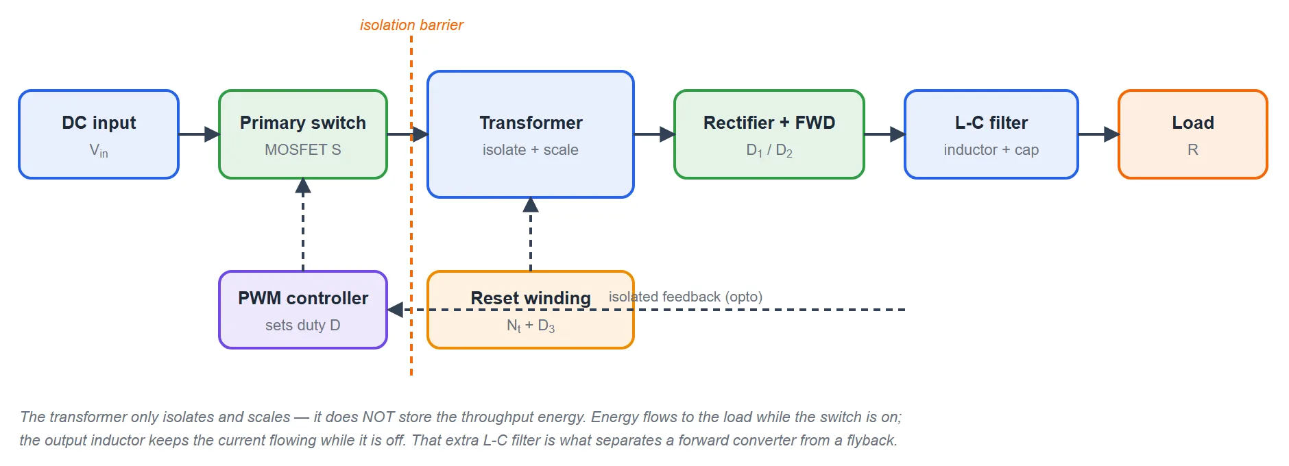
Read it left to right as a power path: the DC input is chopped by the switch, passed through the isolation transformer, rectified by D1, smoothed by the L-C filter, and delivered to the load. Two features mark it as a forward converter rather than a flyback. First, there is a genuine output inductor in the filter — energy is not stored in the transformer, so the inductor is what carries the load through the off-time (with the freewheel diode). Second, a reset winding hangs off the transformer to return the magnetising energy to the source. As in any isolated supply, the feedback crosses the isolation barrier through an opto-coupler so the loop can regulate the output without breaking isolation.
Circuit Diagram & Construction
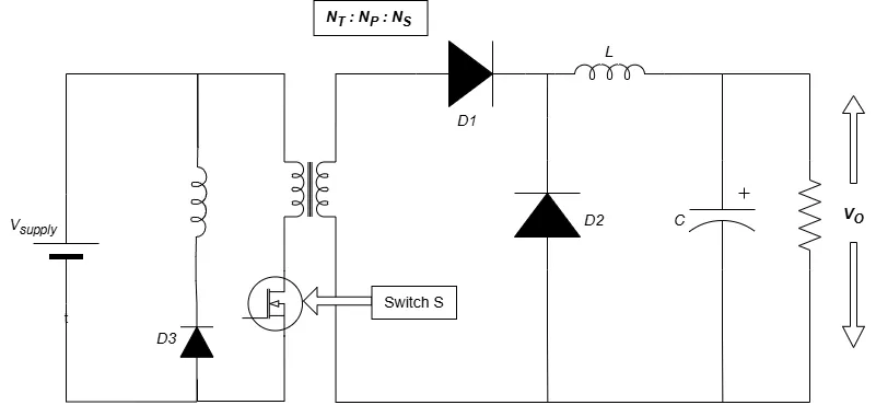
| Transformer (Np : Ns) | Isolates and scales only — an ungapped core with near-zero stored energy in the ideal case. The turns ratio n = Ns/Np sets the secondary voltage during the on-time. |
|---|---|
| Reset winding Nt + diode D3 | The forward converter’s signature part. When the switch opens, the small magnetising current is diverted through Nt and D3 back into the source, resetting the core flux to zero. Without it the core would “walk” into saturation within a few cycles. |
| Switch S (MOSFET) | On the primary, referenced to input ground. Must block Vin(1 + Np/Nt) in the off state — the input plus the voltage reflected from the reset winding. |
| Rectifier diode D1 | On the secondary, in series with Ns. Forward-biased while the switch is on, delivering the scaled voltage n·Vin to the filter. |
| Freewheel diode D2 | Across the filter input (node P). Provides the path for the inductor current while the switch is off — the load current never has to break. This diode is what a flyback does not have. |
| Output filter L, C | A buck-type L-C filter. The inductor L carries a smooth, nearly-DC current (its average equals the load current); the capacitor C only handles the ripple, so output voltage ripple is low. |
Principle of Operation
The switch turns on and off at a fixed frequency; the fraction of each period it stays on is the duty ratio D. The two halves of the cycle share the work between the transformer (which handles the power transfer) and the output inductor (which keeps the load current smooth):
- While S is on the input voltage is applied to the primary, and by the aiding dots a scaled voltage n·Vin appears on the secondary. D1 conducts, so this voltage is applied to the L-C filter and energy flows straight through to the load. The inductor current ramps up as it charges. The reset winding is reverse-biased and idle.
- While S is off the primary and secondary currents fall to zero. The output inductor, however, will not let its current stop — it forces D2 to conduct and freewheels its current back into the load. Meanwhile the transformer’s trapped magnetising energy flows out through the reset winding and D3, returning to the source and demagnetising the core.
So two things happen in parallel during the off-time: the output side freewheels (D2 carrying the inductor current) and the transformer resets (D3 carrying the magnetising current). They are independent. The governing principle for the output is the same volt-second balance on the output inductor as in a buck converter, which fixes Vo; a second volt-second balance, on the transformer core, fixes how much duty the reset winding will allow.
Modes of Operation
A forward converter has two switch states per cycle. Here is each one on the circuit, with the conducting path highlighted.
Mode 1 — Switch ON (powering)
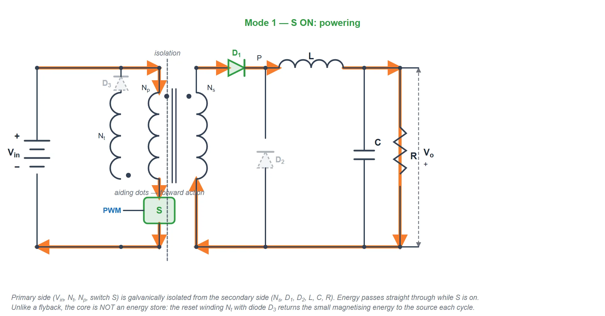
- S is closed, putting the full Vin across the primary. A scaled voltage n·Vin appears on the secondary, forward-biasing D1.
- The voltage applied to the filter is n·Vin; since the output is held at Vo, the inductor sees (n·Vin − Vo) and its current ramps up, delivering power to the load and topping up C.
- The primary carries the reflected inductor current (n·iL) plus a small magnetising current that slowly builds flux in the core. D2 and D3 are both reverse-biased.
Mode 2 — Switch OFF (freewheeling & reset)
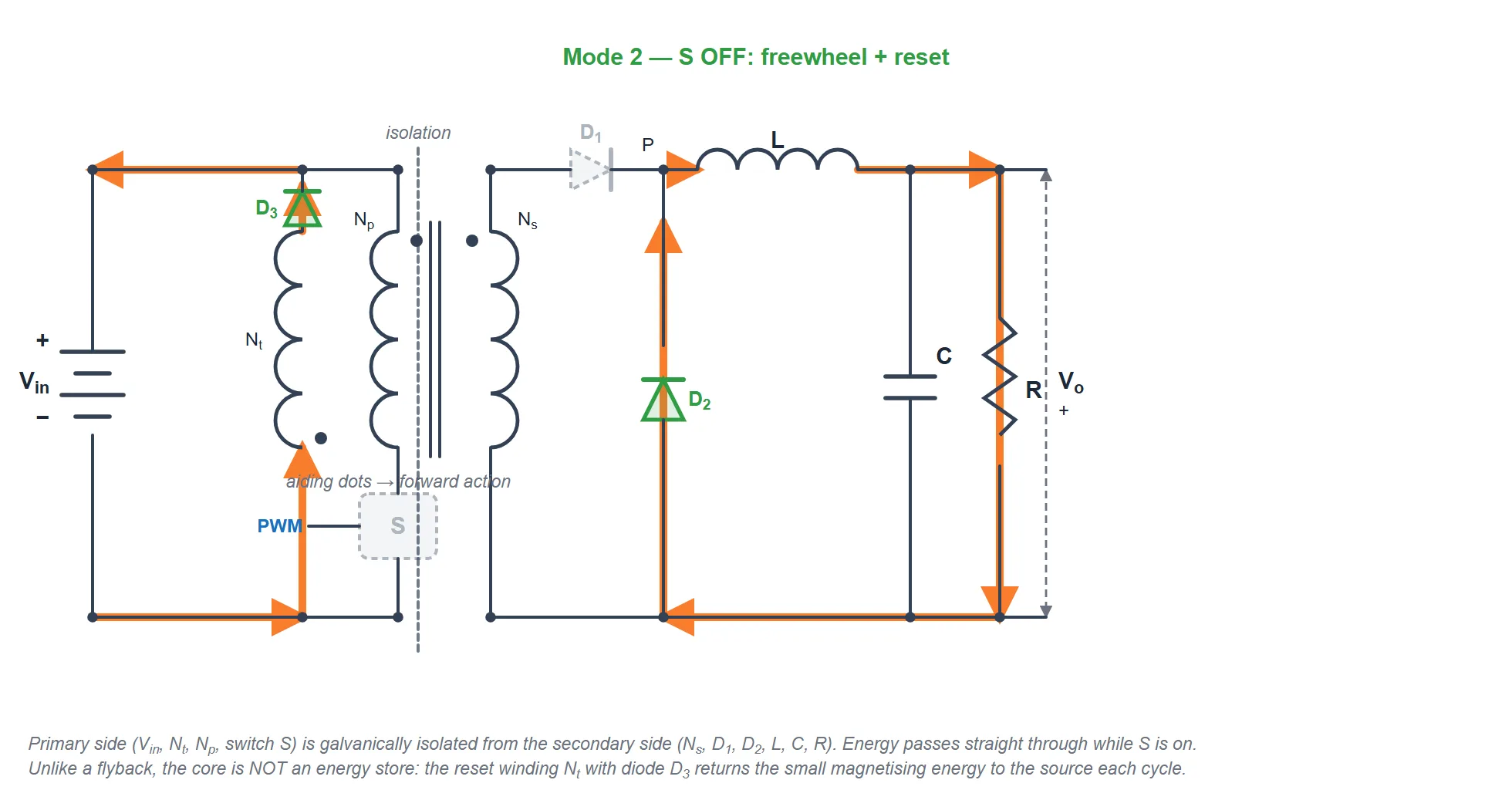
- S opens, so primary and secondary winding currents drop to zero and D1 is reverse-biased — the transformer stops delivering power.
- The output inductor keeps its current flowing, forcing D2 to conduct. The inductor now sees only −Vo, so its current ramps down gently while still feeding the load. This is the freewheeling action of a buck.
- At the same time, the magnetising current trapped in the core is diverted into the reset winding and through D3, flowing against Vin back to the source. This drives the flux down to zero — the core is demagnetised, ready for the next cycle. If this reset does not finish before the switch turns on again, the core saturates.
The Reset Winding & the D ≤ 0.5 Limit
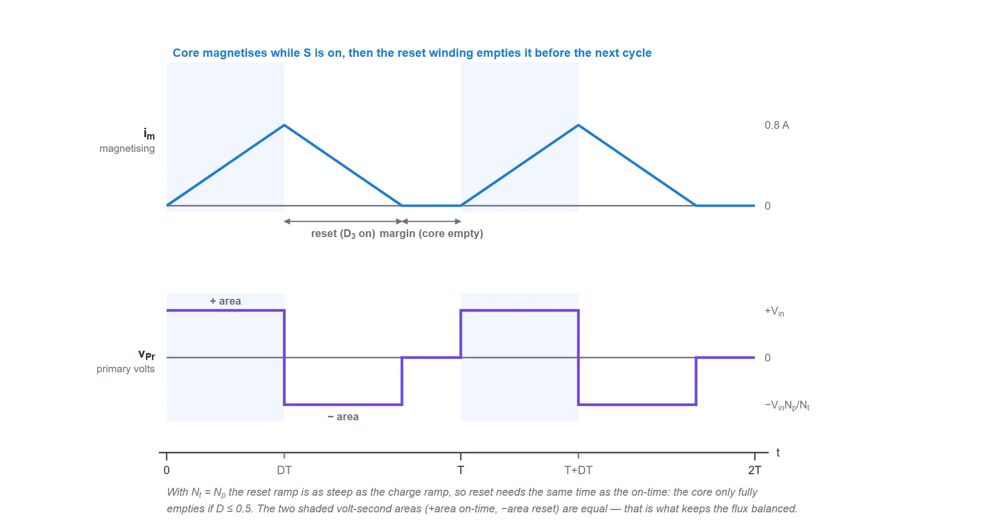
This figure is the heart of the forward converter. The magnetising current (top) is not the load current — it is the small current a real transformer needs to establish flux. It ramps up while the switch is on (slope Vin/Lm), and when the switch opens it is diverted into the reset winding, where it ramps back down to zero as it pushes energy against Vin.
The primary voltage (bottom) tells the story through volt-second balance: over one steady cycle the flux must return to where it started, so the positive volt-seconds applied while the switch is on must be cancelled by the negative volt-seconds during reset. On-time volts are +Vin; reset volts are −Vin·Np/Nt. Setting the areas equal gives the reset time, and therefore the maximum duty ratio:
Vin·D·T = (Vin·Np/Nt)·treset → treset = (Nt/Np)·D·T | Dmax = Np / (Np + Nt)The reset must finish inside the off-time (1−D)T. With the common bifilar design where Nt = Np, the reset ramp is exactly as steep as the charge ramp, so it needs the same time as the on-time — which forces D ≤ 0.5. Push the duty past that and the core never fully resets, the flux walks up cycle by cycle, and the transformer saturates.
Waveforms Explained in Detail
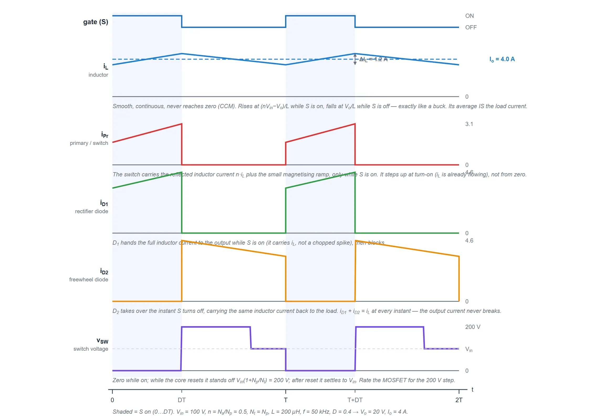
Read the six traces together and the whole converter is visible in one picture:
- Gate. The PWM signal, on for DT and off for (1−D)T. Here D = 0.4, safely under the 0.5 reset limit.
- Inductor current iL. A smooth triangle that never reaches zero — that is continuous conduction. It ramps up at (n·Vin−Vo)/L while the switch is on and down at Vo/L while it is off, exactly like a buck. Its average is the load current, 4 A. This smoothness is the forward converter’s big advantage over the flyback’s burst-fed output.
- Primary / switch current iPr. The reflected inductor current n·iL plus the small magnetising ramp, present only while the switch is on. Notice it steps up at turn-on to a finite value (the inductor is already carrying current), then ramps — it does not start from zero as a flyback’s does.
- Rectifier-diode current iD1. Equal to iL during the on-time, then zero. D1 hands the full, smooth inductor current to the output — not a chopped spike.
- Freewheel-diode current iD2. The mirror image — zero during the on-time, then iL during the off-time. Crucially, iD1 + iD2 = iL at every instant: between them the two diodes carry the inductor current continuously, so the output current never breaks.
- Switch voltage vSW. Near zero while the switch conducts. When it opens, the reset winding clamps the primary and the switch stands off Vin(1 + Np/Nt) = 200 V during the reset interval, then falls to just Vin = 100 V once the core is empty. Size the MOSFET for that 200 V step, not for Vin.
The contrast with the flyback is worth pausing on. There, the two device currents are sharp, tall bursts that never overlap. Here, the inductor current is smooth and shared continuously between D1 and D2. That is the whole reason the forward converter reaches higher power with lower peak currents — the output inductor does the heavy lifting the flyback asks its transformer and capacitor to do.
Key Formulas
All of these come from two volt-second balances — one on the output inductor, one on the transformer core — with n = Ns/Np.
Output voltage (CCM). The inductor sees (n·Vin−Vo) for DT and −Vo for (1−D)T; its average voltage is zero:
(n·Vin − Vo)·D·T = Vo·(1−D)·T → Vo = n · D · VinThis is the buck relation Vo = D·Vin scaled by the turns ratio — a straight line in D, unlike the flyback’s D/(1−D).
Duty ratio for a target output. Rearranging:
D = Vo / (n · Vin)Inductor-current ripple and average. Standard buck filter, using the off-time slope:
ΔiL = Vo·(1−D)·T / L | IL,avg = IoCore reset & duty limit. From flux balance on the transformer:
treset = (Nt/Np)·D·T | Dmax = Np/(Np + Nt) (= 0.5 when Nt = Np)Device voltage stress. Size the switch and the reset diode for the reflected reset voltage:
Switch: VSW,off = Vin(1 + Np/Nt) | D3: VD3,rev = Vin(1 + Nt/Np)(Switch and diode drops, winding resistance and losses are neglected in these ideal expressions; a typical real forward converter is around 80–90% efficient. Eqn. (23.3) of the source lesson matches the output relation above.)
Voltage Gain & Turns Ratio
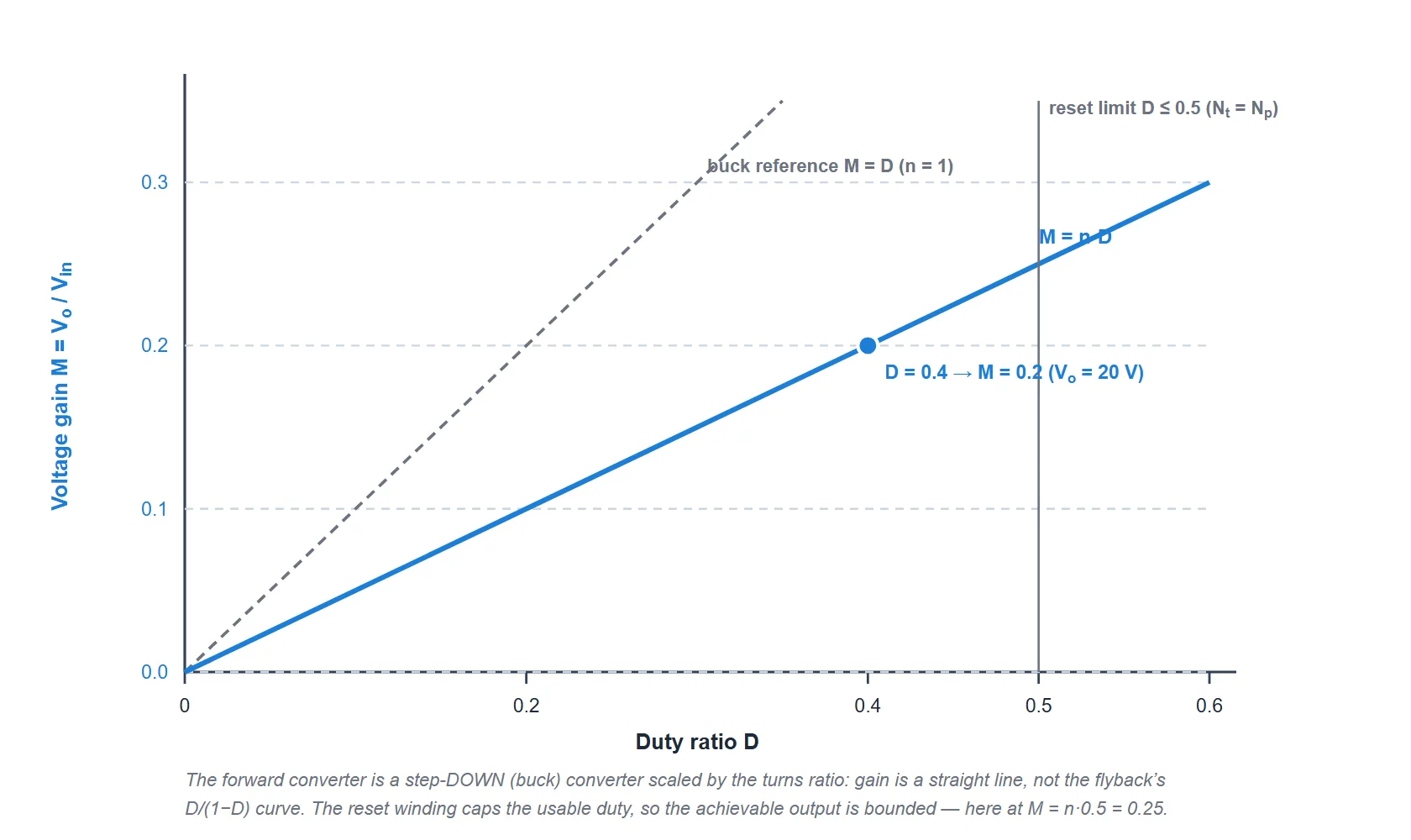
The forward converter’s gain is a straight line, M = n·D — the buck’s M = D tilted by the turns ratio. That makes it easy to control (a linear plant is friendly to a linear controller), but it also means the converter is fundamentally a step-down: the turns ratio, not the duty cycle, does most of the voltage scaling, and the duty only fine-tunes around it. Two consequences follow:
- The turns ratio sets the operating point. An offline supply dropping ~320 V of rectified line to 12 V picks a small n so the duty lands in a comfortable 0.3–0.45 window — safely under the reset limit.
- The reset winding caps the output. Because D cannot exceed Np/(Np+Nt), the maximum achievable gain is n·Dmax. With a 1:1 reset winding that is n·0.5 — a hard ceiling you design the turns ratio around.
- Continuous inductor current keeps it linear. If the load is very light the inductor current can go discontinuous, and then (as in a buck) the output rises above n·D·Vin and becomes load-dependent. Designers size L so the current stays continuous down to ~10 % of rated load.
Worked Example
One consistent design, used by every figure above. Follow the numbers through and the formulas check out.
| Given | Vin = 100 V, Ns:Np = 1:2 (n = 0.5), Nt = Np, D = 0.4, f = 50 kHz (T = 20 µs), L = 200 µH, Lm = 1 mH |
|---|---|
| Output voltage Vo = n·D·Vin | 0.5 × 0.4 × 100 = 20 V |
| Load (for Io = 4 A) R = Vo/Io, Po = VoIo | R = 5 Ω, Po = 80 W |
| Inductor ripple ΔiL = Vo(1−D)T/L | 20 × 0.6 × 20µ/200µ = 1.2 A (Imax = 4.6 A, Imin = 3.4 A → CCM) |
| Magnetising ripple Δim = Vin·D·T/Lm | 100 × 0.4 × 20µ/1m = 0.8 A (small — not load current) |
| Reset time treset = (Nt/Np)·D·T | 1 × 0.4 × 20µ = 8 µs < off-time 12 µs ✓ (4 µs margin) |
| Switch voltage stress Vin(1 + Np/Nt) | 100 × 2 = 200 V |
| Secondary diode stress ≈ n·Vin | 0.5 × 100 = 50 V (D1 and D2) |
| Input current (avg) D·(n·Io) | 0.4 × (0.5 × 4) = 0.8 A → Pin = 100 × 0.8 = 80 W = Po ✓ |
The last row is the sanity check: with no losses, input power equals output power, and it does — 80 W in, 80 W out (the magnetising energy is returned to the source, so it does not appear in the net input power). Notice that D = 0.4 sits comfortably below the 0.5 reset limit, and the reset finishes with 4 µs to spare. Compare this with the flyback worked example at the same 100 V input, 20 V / 4 A output: the forward converter reaches it with a smooth 4 A inductor current instead of a 10.5 A diode burst — the same power, far gentler on the parts.
Forward vs Flyback
They are the two entry-level isolated topologies, and they are opposites in almost every respect. This table is the quickest way to keep them straight:
| Feature | Forward converter | Flyback converter |
|---|---|---|
| Non-isolated parent | Buck (step-down) | Buck-boost (step up or down) |
| Energy transfer | Straight through while switch is ON | Stored while ON, released while OFF |
| Transformer dots | Aiding (diode on during ON) | Opposing (diode off during ON) |
| Core | Ungapped, not an energy store; needs a reset winding | Gapped, stores the throughput energy |
| Output filter | L-C (inductor + capacitor) | Capacitor only |
| Output voltage | Vo = n·D·Vin (linear) | Vo = n·D·Vin/(1−D) |
| Output current | Smooth, continuous (low ripple) | Pulsed, high ripple |
| Duty limit | D ≤ Np/(Np+Nt) ≈ 0.5 | No hard reset limit |
| Typical power | 100–200 W | Up to ~150 W |
| Part count | Higher (extra winding, L, 2nd diode) | Lower (one magnetic part, one diode) |
Advantages & Disadvantages
Advantages
- Smooth, low-ripple output current thanks to the output inductor — the load current never breaks, so output capacitors are smaller and less stressed than a flyback’s.
- Lower peak and RMS currents for a given power, because energy is delivered continuously rather than in bursts. This is why it scales to higher power (~100–200 W) than a flyback.
- Higher efficiency at those power levels, and a smaller, ungapped transformer that does not have to store the throughput energy.
- Galvanic isolation between input and output, as with any transformer-isolated topology.
- Easy to control — the linear Vo = n·D·Vin gain makes the control loop simple, just like a buck.
Disadvantages
- Duty ratio limited to about 50 % (with a 1:1 reset winding), which restricts the usable input-voltage range and the achievable gain.
- High switch voltage stress — Vin(1 + Np/Nt), typically twice the input — because of the reflected reset voltage.
- More parts than a flyback: a third (reset) winding, a second output diode, and an output inductor. The bifilar primary/reset winding is fussy and costly to wind.
- Single-output bias — adding well-regulated multiple outputs is harder than on a flyback, because each needs its own inductor.
- The reset winding wastes a little duty and adds voltage stress; two-switch and active-clamp forward variants exist specifically to relax these limits.
Applications
- Mid-power isolated supplies (100–200 W) — the classic role, above where the flyback becomes inefficient and below where half-bridge and full-bridge take over.
- Desktop and industrial AC-DC adapters and embedded power bricks needing a single, well-regulated isolated rail.
- Telecom and networking DC-DC converters that step a 48 V bus down to board-level rails.
- Battery chargers and LED drivers where a smooth output current is valuable.
- Server and computing auxiliary supplies, and instrumentation supplies that need low output ripple.
- Two-switch and active-clamp forward variants for higher power or higher input voltage, where the basic reset limit and switch stress need to be relaxed.
The rule of thumb: if you need isolation in the 100–200 W range with a clean output, use a forward converter. Below that a flyback is cheaper; above it, a push-pull, half-bridge or full-bridge converter handles the power better.