Phase-Shifted Full-Bridge (PSFB) Converter
The soft-switched full bridge — both legs run at a fixed 50 % and the controller regulates by the phase between them, while the transformer’s leakage inductance resonates with the MOSFET capacitances to switch every device at zero volts. Full drive voltage, Vin-only stress, and almost no switching loss: the workhorse of kilowatt-class isolated supplies.
- Introduction — a full bridge that switches for free
- What is a Phase-Shifted Full-Bridge Converter?
- Block Diagram
- Circuit Diagram & Construction
- Principle of Operation — phase-shift control
- Modes of Operation
- Waveforms Explained in Detail
- Zero-Voltage Switching & the Resonant Tank
- Key Formulas
- Voltage Gain & the Effective Duty
- Worked Example — a 400 V → 48 V / 1 kW stage
- Advantages & Disadvantages
- Applications
- Frequently Asked Questions – FAQs
- Related Topics
Introduction — a full bridge that switches for free
A plain full-bridge converter is already the best high-power isolated topology on paper: four switches drive the transformer with the full ±Vin, yet each switch blocks only Vin. Its one real weakness is switching loss. Every time a MOSFET turns on, it does so with the full bus voltage across it and then dumps the energy stored in its own capacitance as heat. Push the frequency up to shrink the magnetics and that loss grows until it caps the whole design.
The phase-shifted full-bridge (PSFB) keeps the exact same power stage and solves that weakness with nothing but timing. Instead of pulsing the diagonal pairs, it runs both legs at a fixed 50 % duty and regulates the output by sliding the phase of one leg against the other. The reward is that the transformer’s own leakage inductance, working against the MOSFETs’ output capacitances, forms a small resonant tank that swings each switch node to the opposite rail before the device turns on — so it turns on at zero volts. The parasitic that everyone else fights becomes the feature that makes the converter soft-switch.
This page builds the PSFB from that idea: the same two-leg circuit but with its parasitic capacitances and leakage inductor made explicit, what phase-shift control actually does, the four operating intervals in words, why the two legs are not equal (leading vs lagging), the zero-voltage-switching mechanism and its load limit, the formulas, and a realistic 400 V → 48 V kilowatt example.
What is a Phase-Shifted Full-Bridge Converter?
A phase-shifted full-bridge converter is an isolated, soft-switching DC-DC converter: a full-bridge (H-bridge) power stage driven so that every switch turns on under zero-voltage switching (ZVS). It is built from these parts:
- Four MOSFETs in two legs. Leg 1 is S1 (high-side) over S2 (low-side) meeting at node A; leg 2 is S3 over S4 meeting at node B. Both legs sit across Vin, and both run at a fixed near-50 % duty with dead time.
- A body diode and an output capacitance (C1–C4) across each MOSFET. These are not extra parts — they are the device’s own parasitics — but the PSFB uses them: the capacitances are what get charged and discharged to achieve ZVS, and the body diodes clamp each node once it reaches the opposite rail.
- A resonant inductor Lr in series with the primary — mostly the transformer’s leakage inductance, usually topped up with a small discrete inductor. Together with C1–C4 it forms the resonant tank that performs the soft transitions.
- An isolation transformer driven at ±Vin between nodes A and B.
- A full-wave secondary rectifier — on a centre-tapped secondary (Ns1/Ns2) with two diodes D1/D2, or synchronous-rectifier MOSFETs in high-current designs — feeding a buck-type Lo-Co output filter.
The defining trick is the phase shift. When the two legs switch in phase, both ends of the primary move up and down together, vAB stays at zero, and no power flows. As leg 2’s timing slides against leg 1’s, a window opens in which one node is high while the other is low, and the primary sees ±Vin for exactly that overlap. The phase shift is the effective duty cycle.
Block Diagram
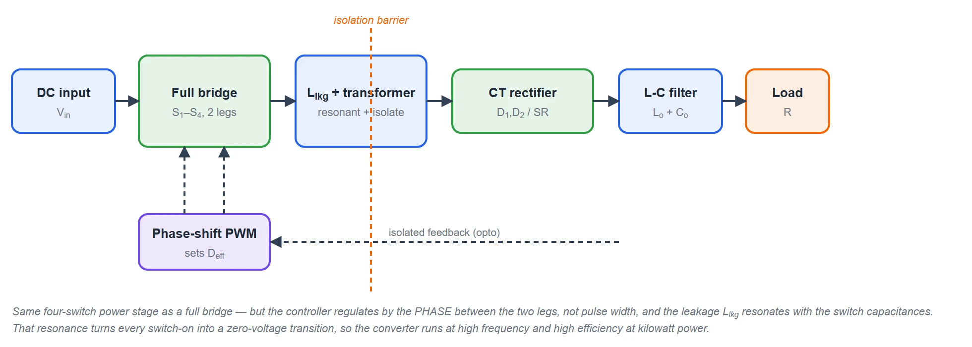
Read it as a power path: the DC bus is chopped by the four-switch bridge, driven through the resonant inductor and transformer, rectified, smoothed by the L-C filter, and delivered to the load. Two things mark it as phase-shifted. First, the controller does not vary pulse width — it sets the phase between the two legs, which fixes the effective duty Deff. Second, the leakage inductor is drawn as a real element, because here it is a working part of the circuit, not a nuisance. Feedback crosses the isolation barrier through an opto-coupler as usual.
Circuit Diagram & Construction
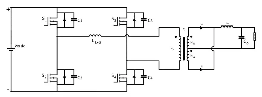
This is the power stage, drawn and labelled in our own schematic style. It is the same H-bridge as a hard-switched full bridge, but two normally-hidden details are made explicit because the PSFB depends on them. Tracing it across:
| Switch legs S1/S2 (leading) and S3/S4 (lagging) | Two legs directly across Vin, making switching nodes A and B. Within each leg the two switches are complementary at a fixed ~50 % duty; across the bridge, diagonal pairs deliver power. The gating of leg S3/S4 is phase-shifted against leg S1/S2. Each switch blocks only Vin. |
|---|---|
| Body diodes + output capacitances C1–C4 | Every MOSFET’s intrinsic body diode and output capacitance (Coss). They are drawn here because the PSFB relies on them: the capacitances are charged and discharged during the dead time to reach zero voltage, and the body diode conducts the moment a node arrives at the opposite rail, holding it there until the gate turns on. |
| Leakage inductor Llkg (the resonant inductor) | An inductor in series with the primary that emphasises the transformer’s leakage inductance — often just the leakage itself, sometimes topped up with a small discrete inductor. With C1–C4 it forms the resonant tank that swings the switch nodes. A larger Llkg stores more energy and so extends ZVS to lighter loads. (It is written Lr in the formulas below.) |
| Transformer T1 (primary Np, centre-tapped secondary Ns1/Ns2) | Driven between nodes A and B at ±Vin. Symmetric AC drive — the core swings both ways, so no reset winding and no air gap are needed. The secondary is centre-tapped: the tap is the output return, and each half-winding feeds the output on one half-cycle. |
| Rectifier D1, D2 (or SR MOSFETs) | A two-diode centre-tapped rectifier: D1 conducts from Ns1 on the positive half-cycle, D2 from Ns2 on the negative, so only one diode drop sits in the output path. High-current designs replace the diodes with synchronous-rectifier MOSFETs. Each device blocks about 2·n·Vin. |
| Output filter Lo, Co | A buck-type L-C filter, fed twice per period, so its inductor current ripples at twice the switching frequency. |
Principle of Operation — phase-shift control
Both legs free-run at a fixed ~50 % duty, so every node swings rail-to-rail every period no matter what. The only control variable is the phase between them:
- Legs in phase. Nodes A and B rise and fall together. The voltage across the primary, vAB = vA − vB, stays at zero the whole period — no power reaches the output.
- Legs shifted. Slide leg 2 later in time and a window opens where node A is already high while node B is still low (and half a period later, the mirror). During that overlap vAB = ±Vin and power flows. The wider the phase shift, the wider the overlap.
- Legs fully anti-phase. Maximum overlap — the primary is driven for almost the whole period, the largest output.
So the phase shift behaves exactly like a duty cycle: call the overlap fraction of the period per pulse D, and the effective duty Deff = 2D. Between the overlaps the bridge parks both ends of the primary on the same rail — a freewheeling interval where vAB = 0. The output then follows from volt-second balance on the output inductor, just as in a buck: the transformer only scales the pulse height by n. Crucially, because every node always completes a full rail-to-rail swing during the dead time, the circuit gets its zero-voltage transitions automatically — which is the subject of the ZVS section below.
Modes of Operation
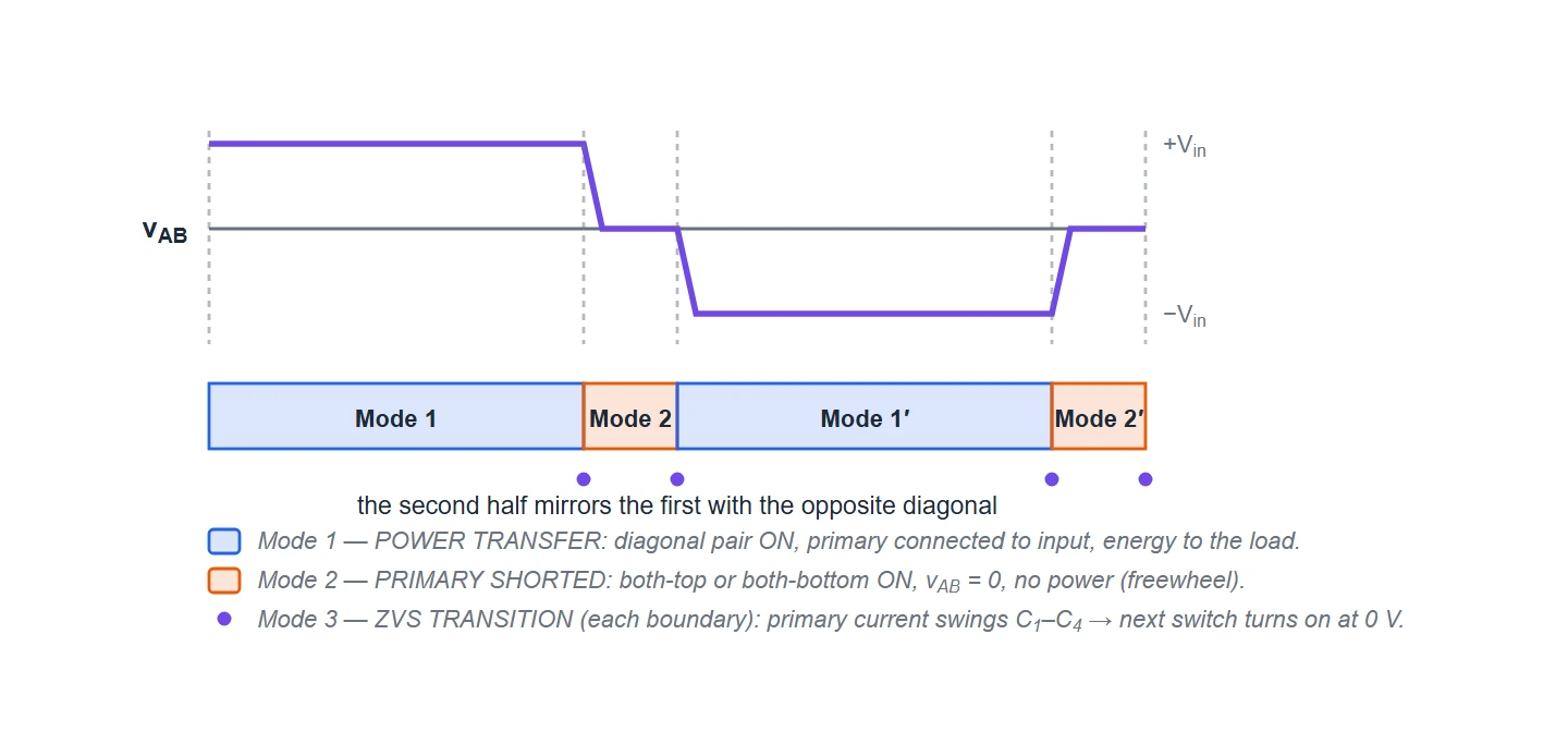
Reading the operation directly off the power circuit of Figure 2, the two legs each switch complementarily at a fixed 50 % duty with a short dead time, and the gating of leg S3/S4 is phase-shifted against leg S1/S2. That phase shift does two jobs: it allows the zero-voltage-switching transitions, and it ensures the transformer primary is at any instant either connected to the input or shorted. From those two conditions the converter has just three operating states, which the map below lines up against the bridge voltage vAB.
Mode 1 — Power transfer (diagonal switches ON)
- When the diagonal switches are on, power is transferred to the load through the transformer secondary. Take S1 (top of leg 1) and S4 (bottom of leg 2): current runs from the + rail through S1 to node A, through Llkg and the primary to node B, and down through S4 to the − rail. The primary is connected to the input and sees the full Vin.
- On the centre-tapped secondary the induced voltage forward-biases D1 (from Ns1), the output inductor Lo charges, and energy flows to the load. Half a period later the opposite diagonal (S2 + S3) reverses the primary voltage and D2 (from Ns2) conducts — the same power transfer with the opposite polarity.
- The two off switches are each clamped by their own leg to Vin, so their output capacitances are charged to Vin, ready for the next transition.
Mode 2 — Primary shorted / freewheel (both-top or both-bottom ON)
- If either the top switches or the bottom switches of both legs are on at the same time, no power is transferred to the secondary, because zero voltage is applied across the primary. Both ends of the primary sit on the same rail, so vAB = 0 and the transformer primary is effectively shorted.
- The primary current does not stop — it keeps circulating around that shorted loop (through the two conducting switches and Llkg), providing the stored inductive energy that the next transition will use.
- On the secondary, with no transformer voltage the rectifier devices carry the output-inductor current and Lo freewheels into the load — the output is never interrupted, exactly like a buck’s freewheel interval.
Mode 3 — Zero-voltage transition (diagonal switches turn OFF)
- When the conducting diagonal switches are turned off, the primary current flows into the output capacitors of the respective MOSFETs, moving each switch’s drain voltage toward the opposite input rail. When the incoming device reaches the far rail, its voltage is zero, so it turns on under ZVS and its body diode holds the node there until the gate rises.
- This works only when there is enough circulating current — enough inductive stored energy — to charge and discharge those capacitances. The parasitic output capacitances C1–C4 and the leakage inductance Llkg act together as a resonant tank: during the transition the energy stored in Llkg swings the node capacitance to reach zero voltage at turn-on.
- Because it is the circulating current that must do this, the leakage inductance is not minimised — a larger resonant inductance provides ZVS over a greater load range, and extra leakage can even be added deliberately. This is also why ZVS weakens at light load, where the circulating current is small.
Waveforms Explained in Detail
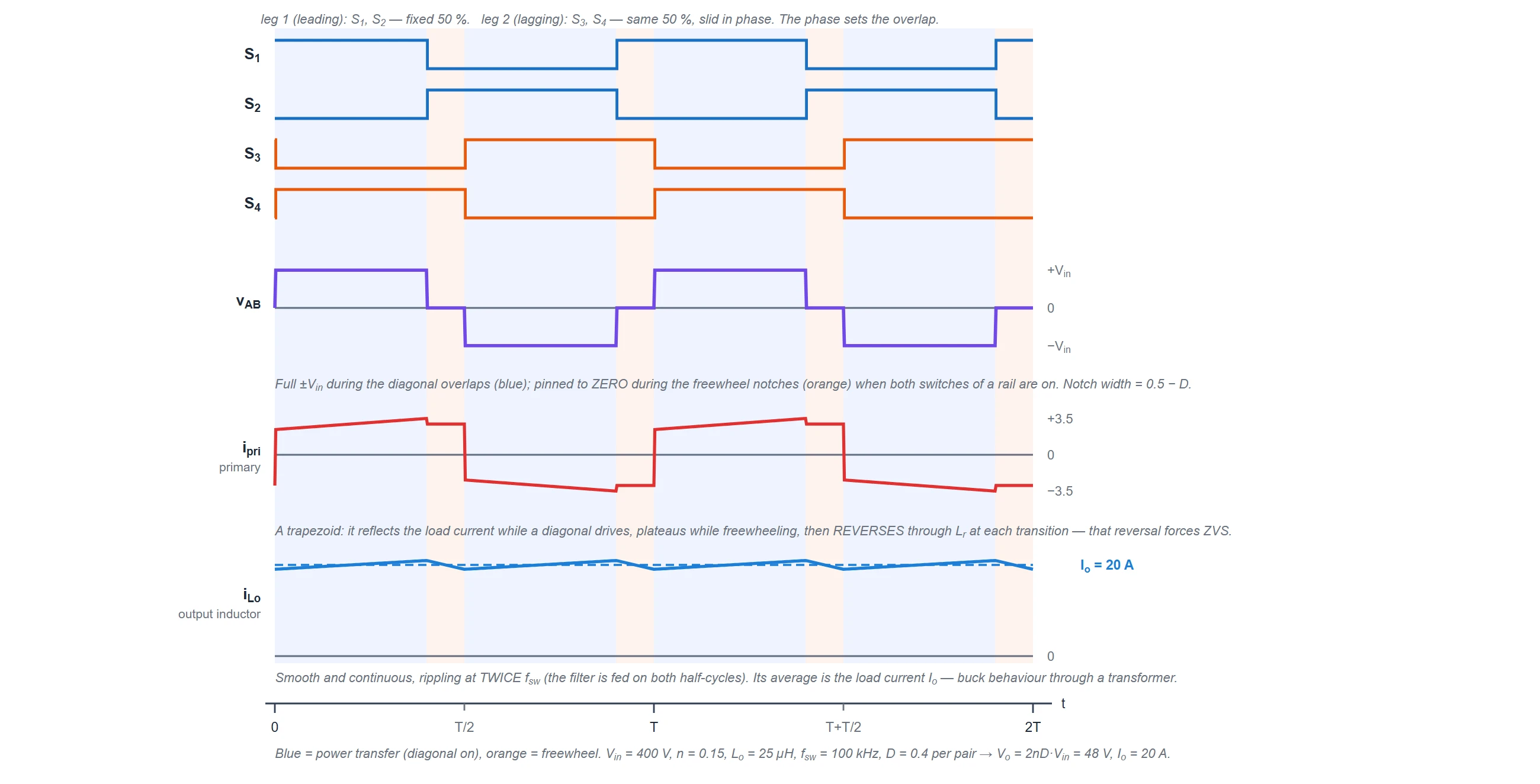
Read the traces together and the whole converter is visible in one picture:
- Gates. Leg 1 (S1, S2) and leg 2 (S3, S4) both run a fixed 50 % square wave with dead time. Leg 2 is slid in phase; the amount of slide sets how much the diagonals overlap, and that overlap is the power-transfer time.
- Bridge voltage vAB. The full ±Vin during each diagonal overlap (blue), and pinned to zero during the freewheel notches (orange) when both ends of the primary sit on the same rail. Widening the phase widens the ±Vin pulses and shrinks the notches.
- Primary current ipri. The signature PSFB trapezoid. While a diagonal drives, it carries the reflected load current (rising with iLo); while freewheeling, it plateaus and decays slowly; at each transition it reverses through Lr — and that reversal current is precisely what charges and discharges the MOSFET capacitances to make ZVS happen.
- Output inductor current iLo. A smooth triangle rippling at twice the switching frequency, because the filter is topped up on both half-cycles. Its average is the load current — buck behaviour through a transformer.
Notice that the interesting action is all at the edges: the flat tops carry the power, but the transitions — where vAB steps and ipri reverses — are where the soft switching is won or lost.
Zero-Voltage Switching & the Resonant Tank
This is the whole reason the PSFB exists, so it is worth slowing down. During each dead time the switch that is about to turn on has its output capacitance charged to Vin. If it were simply gated on, that stored energy (½CossVin²) would dump through the channel as heat, every transition, every device. The PSFB avoids it by making the primary current do the discharging first.
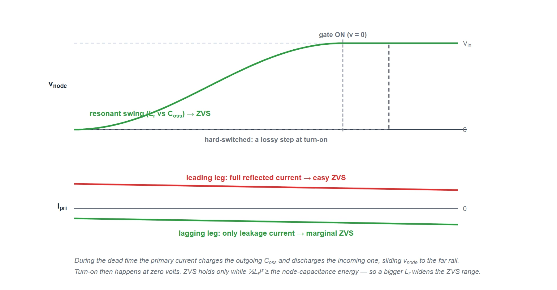
Here is the mechanism, one step at a time. When a conducting switch turns off, the primary current has nowhere to go but into the switch-node capacitances: it charges the outgoing device’s Coss and discharges the incoming one. Because Lr and those capacitances form an L-C tank, the node voltage does not step — it slides along a smooth (cosine) arc from one rail toward the other. If there is enough energy in Lr, the node reaches the opposite rail, the incoming device’s body diode clamps it there, and the gate is turned on while the drain-source voltage is already zero. Turn-on loss essentially vanishes.
The condition for it to work is an energy balance — the inductor must hold at least enough energy to swing the node capacitance across the full bus:
½ · Lr · i² ≥ ½ · Ceq · Vin² (Ceq = the effective node capacitance being swung)That single inequality explains the PSFB’s personality:
- The leading leg soft-switches easily. It transitions right at the end of the power interval, when i is the full reflected load current — plenty of energy, ZVS holds down to light load.
- The lagging leg is the hard one. It transitions during freewheeling, when only the decayed leakage current remains. At light load that current — and its energy — can be too small, the node never reaches the far rail, and ZVS is lost (the switch turns on partially hard).
- Bigger Lr buys a wider ZVS range. More inductance stores more energy for the same current, so ZVS holds to a lighter load — the direct trade for the small duty-cycle loss Lr also causes. Designers size Lr for the lightest load at which ZVS is still required.
Well designed, a PSFB with synchronous rectification runs at 90–95 % efficiency at high switching frequency, with the switch voltage stress held to Vin and no snubber circuits needed — the resonant tank does the job a snubber otherwise would, but without burning the energy.
Key Formulas
All from volt-second balance on the output inductor, with n = Ns/Np and D the overlap (power-transfer) duty of each diagonal pair as a fraction of the full period (D ≤ 0.5). Deff = 2D is the fraction of the period the secondary carries voltage.
Output voltage (CCM). The filter is fed n·Vin for 2D of the period and 0 for the rest:
(n·Vin − Vo)·2D·T = Vo·(1 − 2D)·T → Vo = 2 · n · D · Vin (= n · Deff · Vin)Here D is set by the phase shift, not by pulse width — that is the only structural change from a hard-switched full bridge.
Phase / effective duty for a target output. Rearranging:
Deff = Vo / (n · Vin) (0 ≤ Deff ≤ 1; command a little extra to cover duty-cycle loss)Inductor-current ripple and average. Standard buck filter, ripple repeating every half period:
ΔiLo = (n·Vin − Vo)·D·T / Lo | ILo,avg = IoDevice stress. Each off switch is clamped by its own leg; each rectifier device sees the secondary pulse:
Switch: VS,off = Vin | Rectifier (centre-tapped): VD,rev = 2 · n · VinCurrents. The primary carries the reflected load current at full drive voltage:
Ipri ≈ n · Io | Iin,avg = 2 · D · n · Io = Po / VinZVS energy condition (the lagging leg is the binding case):
½ · Lr · i² ≥ ½ · Ceq · Vin² → raise Lr (or the min load) until it holds at your lightest ZVS load(Switch and diode drops, winding resistance and core losses are neglected. A well-designed phase-shifted full bridge with synchronous rectifiers typically reaches 90–95 % efficiency at high frequency, with no dissipative snubbers.)
Voltage Gain & the Effective Duty
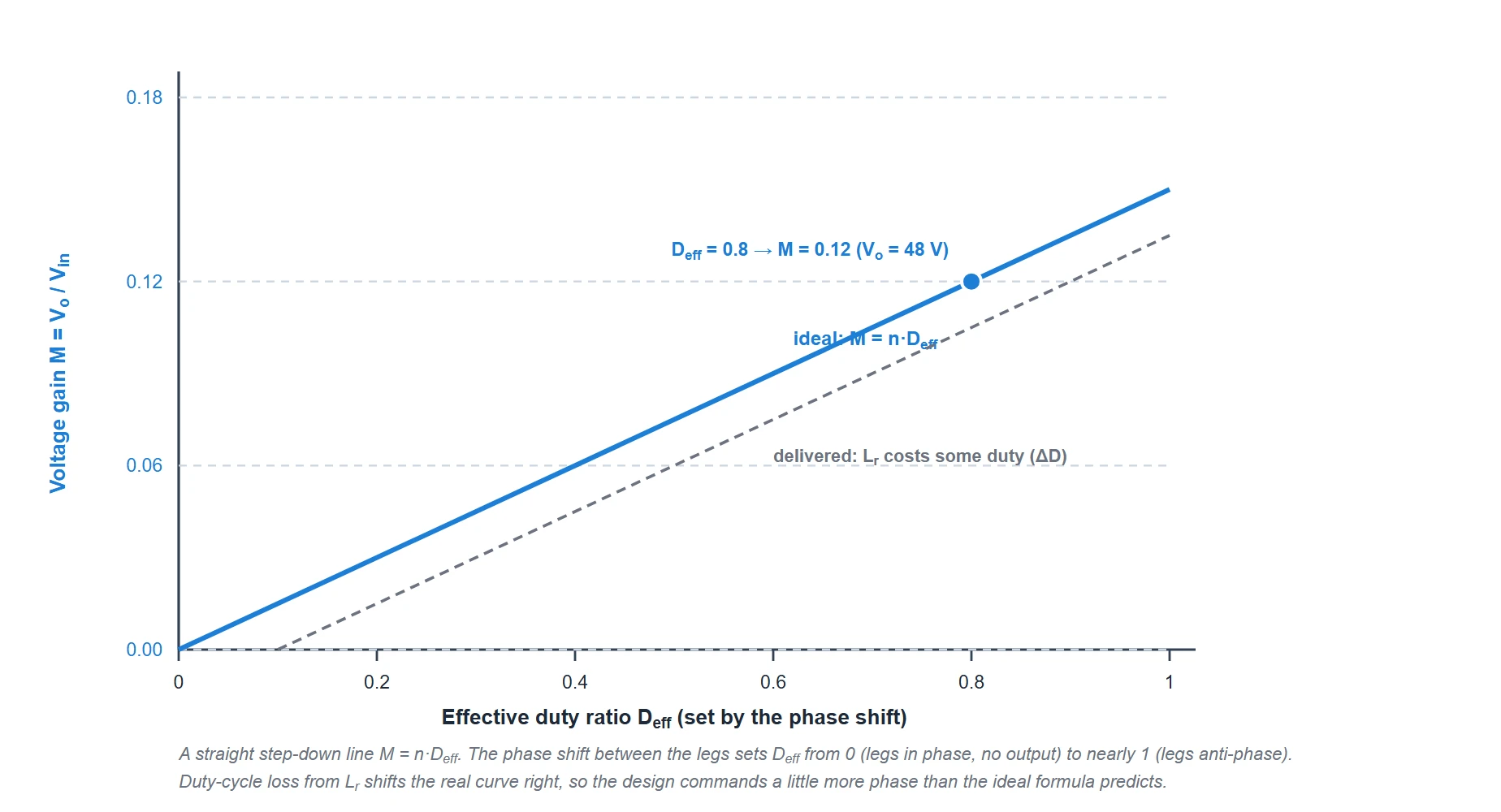
The PSFB’s gain is a straight line, M = n·Deff, with Deff ranging from 0 (legs in phase, no output) to nearly 1 (legs anti-phase). Like all its buck-derived relatives it is fundamentally a step-down through a transformer. Key points:
- The turns ratio does the coarse scaling. Here n = 0.15 puts the 400 V → 48 V operating point at a comfortable Deff = 0.8, leaving phase headroom for line and load regulation.
- The phase shift is the fine control. The controller trims Deff to hold Vo as the input bus and load move — no change in switching frequency, so the magnetics stay optimally sized.
- Duty-cycle loss shifts the real curve. While Lr reverses the primary current at each transition, the transformer momentarily sees no voltage, so the delivered Deff is a little less than commanded — the dashed line. The design simply commands slightly more phase to compensate.
Worked Example — a 400 V → 48 V / 1 kW stage
One consistent design, used by every figure above — a realistic telecom/server rectifier stage. Follow the numbers and the formulas check out.
| Given | Vin = 400 V, n = Ns/Np = 0.15, D = 0.4 per pair, f = 100 kHz (T = 10 µs), Lo = 25 µH, Lr = 6 µH, Lm = 2 mH |
|---|---|
| Primary swing ±Vin | ±400 V (full bus, both directions) |
| Effective duty Deff = 2D | 0.8 (set by the phase shift) |
| Output voltage Vo = 2·n·D·Vin | 2 × 0.15 × 0.4 × 400 = 48 V |
| Load (for Io = 20 A) R = Vo/Io, Po = VoIo | R = 2.4 Ω, Po = 960 W (≈ 1 kW) |
| Secondary pulse voltage n·Vin | 0.15 × 400 = 60 V (applied Deff = 0.8 of the period) |
| Inductor ripple ΔiLo = (n·Vin−Vo)·D·T/Lo | (60−48) × 0.4 × 10µ/25µ = 1.92 A at 2f (Imax 20.96, Imin 19.04 → CCM) |
| Magnetising swing Δim = Vin·D·T/Lm | 400 × 0.4 × 10µ/2m = 0.8 A bipolar (±0.4 A) |
| Switch voltage stress Vin | 400 V (each MOSFET blocks only the bus) |
| Rectifier reverse voltage 2·n·Vin (centre-tapped) | 2 × 0.15 × 400 = 120 V (secondary pulse n·Vin = 60 V) |
| Primary current (driving) ≈ n·Io | ≈ 3 A (peak ≈ 3.5 A with magnetising) |
| Input current (avg) 2·D·n·Io | 2 × 0.4 × 0.15 × 20 = 2.4 A → Pin = 400 × 2.4 = 960 W = Po ✓ |
The last row is the lossless sanity check: 960 W in, 960 W out. In a real converter the difference between this ideal and the measured 90–95 % efficiency is almost entirely conduction loss (the switching loss is what ZVS removed). To secure ZVS on the lagging leg down to, say, a quarter load, the designer would check ½Lri² against ½CeqVin² at that current and, if short, raise Lr — accepting the small duty-cycle loss that comes with it.
Advantages & Disadvantages
Advantages
- Zero-voltage switching for free. The turn-on switching loss essentially disappears, using only the leakage inductance and the MOSFETs’ own capacitances — no dissipative snubbers.
- High frequency and high efficiency together. Removing switching loss lets the converter run fast (shrinking the magnetics) while still reaching 90–95 % efficiency.
- Full-bridge stresses. Full ±Vin primary drive, yet each switch blocks only Vin — and the primary current is low, so it scales to kilowatts.
- Simple, fixed-frequency control. Regulation is by phase shift at a constant frequency, which is easy to filter and EMI-plan for — a practical edge over variable-frequency resonant converters.
- Isolation and clean output, like any transformer-isolated buck-derived converter.
Disadvantages
- ZVS is load-dependent. The lagging leg loses ZVS at light load, where it hard-switches again; controllers manage this with adaptive dead time, a bigger Lr, or burst modes.
- Duty-cycle loss from Lr shaves the effective duty, forcing a little more phase / turns ratio.
- Four switches and two floating gate drives plus a carefully tuned dead time — more complex than a single-ended converter, overkill below a few hundred watts.
- Secondary-side ringing. The leakage inductor resonating with rectifier capacitance can ring on the secondary, sometimes needing a clamp or snubber there.
- No built-in flux balancing in the basic circuit — volt-second imbalance can walk the core, so designs use current-mode control or a small series blocking capacitor.
Applications
- Telecom and server rectifiers — the classic home of the PSFB, e.g. a 48 V / 1–3 kW stage behind a PFC front end.
- EV on-board chargers and DC fast-charging modules, where high efficiency at kilowatt scale is decisive.
- Industrial and battery-charging supplies — welding, plating, high-power chargers.
- Renewable-energy converters — isolated DC-DC stages in solar and energy-storage systems.
- Any high-power isolated DC-DC stage where switching loss would otherwise cap the frequency and the efficiency.
The PSFB is the natural next step from the plain full-bridge converter: identical power stage, but a smarter drive that trades a little control and design effort for a large cut in switching loss. Where efficiency and frequency matter above a few hundred watts, it is the default choice — with resonant topologies (LLC and the like) taking over only when even softer switching or a wider range is needed.
Frequently Asked Questions – FAQs
Related Topics
- Full-Bridge Converter — the hard-switched parent power stage
- Half-Bridge Converter — the split-rail two-switch bridge
- Push-Pull Converter — the dual-switch isolated buck
- Active-Clamp Forward — single-ended ZVS converter
- Series Resonant Converter — the resonant next step
- Forward Converter — the single-switch isolated buck
- DC-DC Converters — Overview
- MOSFET — the usual bridge switch
- All Power Electronic Converters