Buck Converter
The primary function of a buck converter is to step down voltage from a higher level to a lower level.
DC-DC Converter
DC-DC converters are integral electronic circuits that serve a crucial function in contemporary power management systems. Their primary role involves converting the voltage of a direct current (DC) source from one level to another, ensuring stable and efficient power distribution to diverse electronic devices and systems. In scenarios where input voltage levels may fluctuate due to factors such as battery discharging over time or alterations in load conditions, DC-DC converters uphold a consistent output voltage, delivering reliable power to the system's components. A noteworthy advantage of these converters lies in their superior power conversion efficiency. Through the implementation of switching techniques, they can minimize power losses associated with resistive elements, such as transformers or linear regulators, which typically produce heat and squander energy. Consequently, this approach leads to enhanced overall efficiency and prolonged battery life in portable devices.
DC-DC converters are widely employed in various applications, including power supplies for computers, mobile devices, electric vehicles, and renewable energy systems. They play a pivotal role in ensuring that electronic devices receive the appropriate voltage levels required for optimal performance. By efficiently converting and regulating DC voltages, these converters contribute to the overall reliability and functionality of modern electronic systems.
What is DC-DC BUCK CONVERTER?
The Buck Converter is a specialized type of direct current (DC) to direct current (DC) converter that is engineered to efficiently step down the applied DC input voltage. This means that it is designed to decrease a fixed DC input to a specific DC output voltage, ensuring that the output voltage is consistently lower than the input voltage. Due to this characteristic, the Buck converter is often referred to as a step-down converter or a step-down chopper.
The efficient power conversion achieved by a buck converter is instrumental in prolonging battery life and minimizing heat dissipation , rendering it particularly advantageous for the operation of compact electronic devices. Its applicability spans across a diverse array of contexts and it is widely integrated into switched-mode power supplies (SMPS) where a lower output DC voltage is necessitated in comparison to the input DC voltage.
The Buck converter is a versatile and efficient solution for voltage regulation in various electronic applications, making it a fundamental component in modern power electronics.
Working Principle of Buck Converter
The buck converter functions by utilizing the principle of storing energy in an inductor. When an electric current flows through the inductor, the voltage drop across it is directly proportional to the rate of change of the current. A switching transistor is employed to alternate rapidly between on and off states, creating a high-frequency switching action between the input and output. This enables the circuit to sustain a continuous output by harnessing the energy stored in the inductor.
The circuit diagram for a typical buck converter is shown in the figure below.
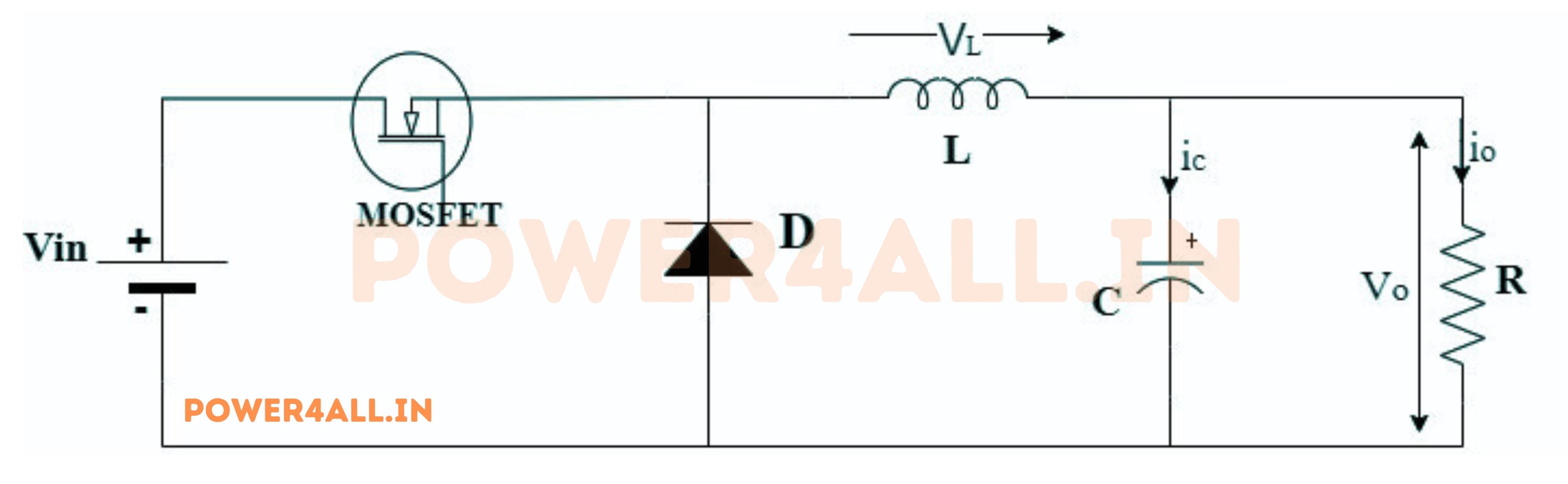
In this circuit, the input voltage is linked to a controllable solid-state device functioning as a switch. The circuit diagram depicts this switch as a power MOSFET. Another essential component in the circuit is a freewheeling diode (FD). The switch and the FD are interconnected with a low-pass LC filter to diminish current and voltage ripples, thereby facilitating the production of a regulated DC output.
In this scenario, the load is exclusively resistive. Both the input voltage and current across the load remain constant, thus allowing the load to be regarded as a current source.
The controlled switch is activated and deactivated through the utilization of Pulse Width Modulation (PWM). PWM can be categorized as either time-based or frequency-based. Time-based modulation is predominantly employed in buck converters due to its straightforward construction and application. This form of modulation maintains a constant frequency. In contrast, frequency-based modulation encompasses a broad spectrum of frequencies to facilitate precise switch control and necessitates a complex design for the low-pass LC filter.
The buck converter operates in two distinct modes, which are determined by the state of the switch. The first mode occurs when the switch is closed, allowing current to flow through the inductor. The second mode occurs when the switch is open, and the inductor discharges its stored energy through the load. The operation of the buck converter can be divided into two modes, which are as follows:
Mode-1 when Diode is forward-biased
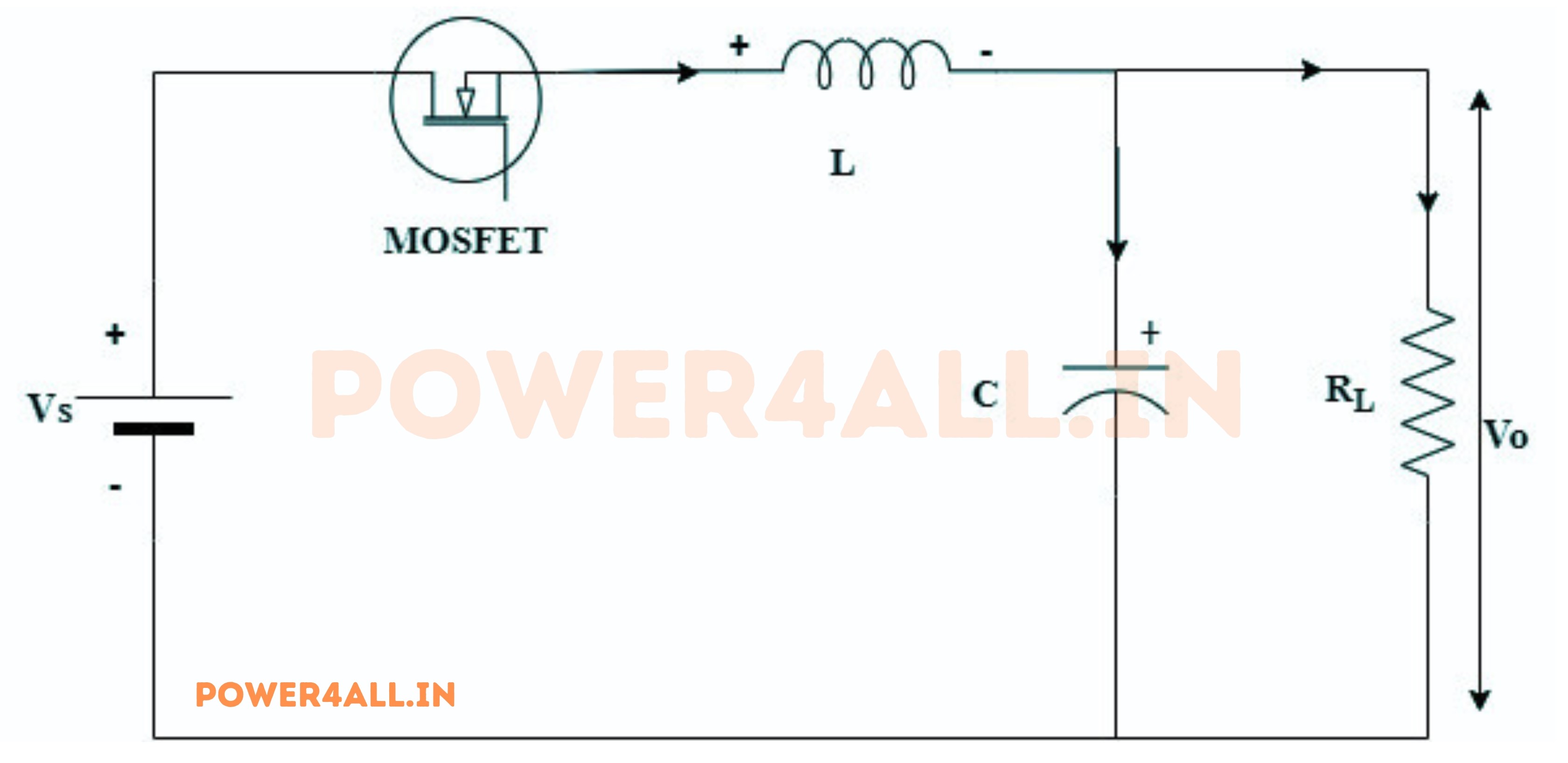
In this operational mode, switch S1 is in the closed state (ON), while diode FD is in the open state (OFF), thereby permitting the passage of current through switch S1. The corresponding circuit diagram is depicted in the above figure.
When a constant direct current (DC) voltage is applied across the input terminal of the circuit, current flows through the closed switch S1, while the diode FD is in a reverse-biased condition. Consequently, the inductor "L" stores energy in the form of a magnetic field. The capacitor, as indicated in the circuit diagram, also experiences current flow, leading to the storage of charge. The voltage across the capacitor is then manifested across the load and equals the output voltage Vo.
- Switch (S) is On When the switch is closed, the input voltage 𝑉𝑖𝑛Vin is directly applied to the inductor (L).
- Inductor Behavior The inductor current increases linearly, storing energy in the magnetic field. The voltage across the inductor is 𝑉𝐿=𝑉𝑖𝑛−𝑉𝑜𝑢𝑡 .
- Diode (D) The diode is reverse-biased and does not conduct.
- • Output Voltage (Vout) During this period, the output capacitor (C) provides current to the load, maintaining the output voltage.
- • Energy Storage The energy is stored in the inductor and capacitor, and the output voltage is lower than the input voltage.
Mode-2 when Diode is reverse-biased
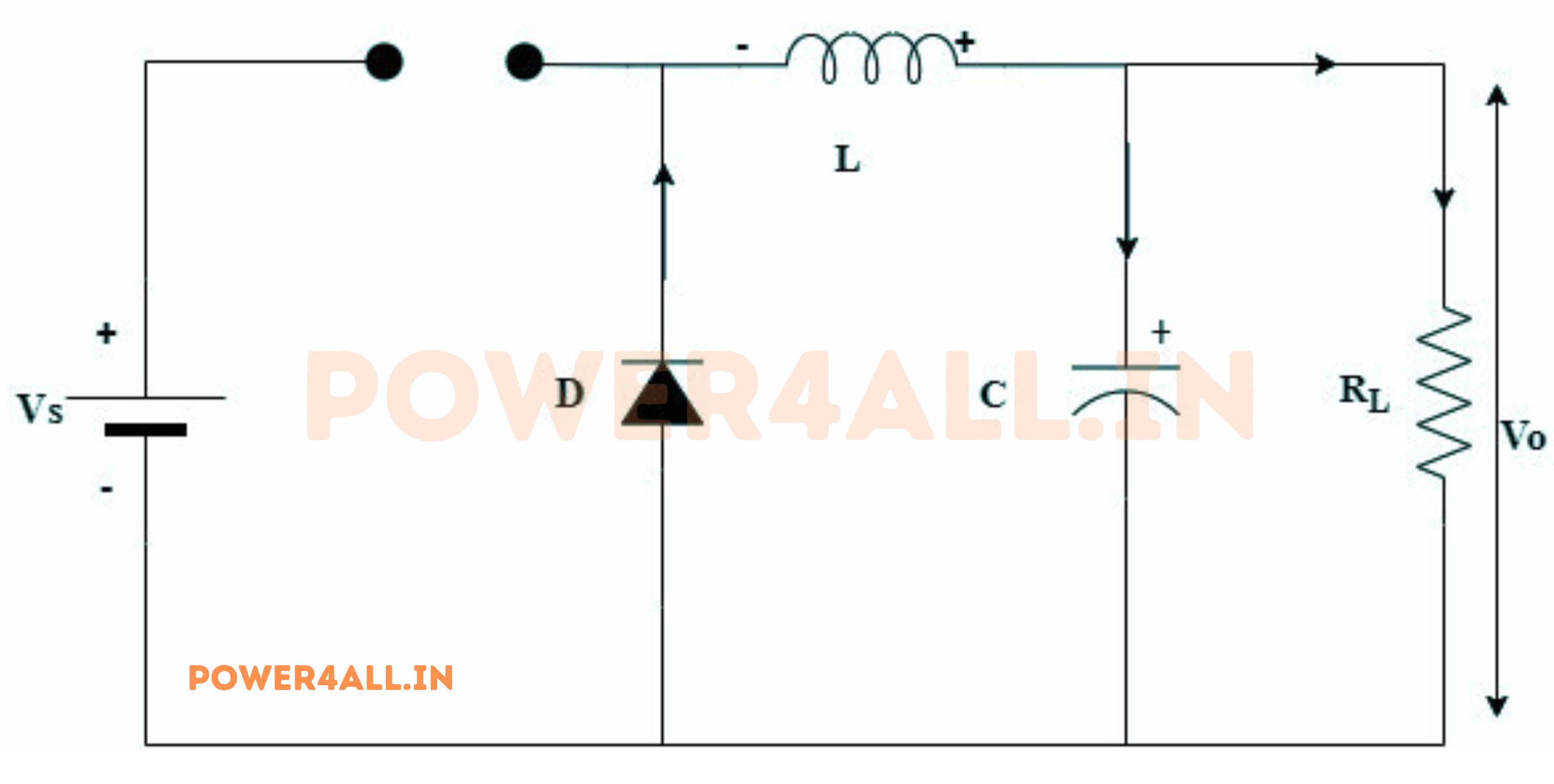
During the operation, switch S1 remains in an open (OFF) state, while diode FD is in a closed (ON) state. As a result, diode FD facilitates the flow of current, whereas switch S1 impedes the current flow. The circuit diagram illustrating this mode is depicted in the above figure.
When the switch S1 is open, the inductor in the circuit functions as an energy storage component by creating a magnetic field. In this state, the inductor acts as the source, leading to the closure of diode FD. During this phase, the inductor discharges the previously stored energy from the closed switch S1 mode. As the inductor releases energy, its polarity reverses, causing the freewheeling diode (FD) to become forward biased and facilitating the flow of current through the circuit. The direction of current flow is illustrated in the accompanying figure.
The flow of current within the circuit will persist until the stored energy in the inductor is fully dissipated. Upon complete discharge of the inductor, the freewheeling diode (FD) will enter a reverse biased state, causing diode FD to transition to an open condition. Subsequently, switch S1 will promptly close, thereby perpetuating the cycle.
- Switch (S) is Off: When the switch is open, the inductor maintains the current flow due to its stored energy, causing the inductor voltage to reverse.
- Inductor Behavior: The current flows through the diode (D) and the load. The inductor current decreases linearly.
- Diode (D): The diode becomes forward-biased and conducts current from the inductor to the load.
- Load (R): The load receives current from the inductor through the diode, maintaining the output voltage.
- Output Voltage (Vout): During this period, the output capacitor (C) provides current to the load, maintaining the output voltage.
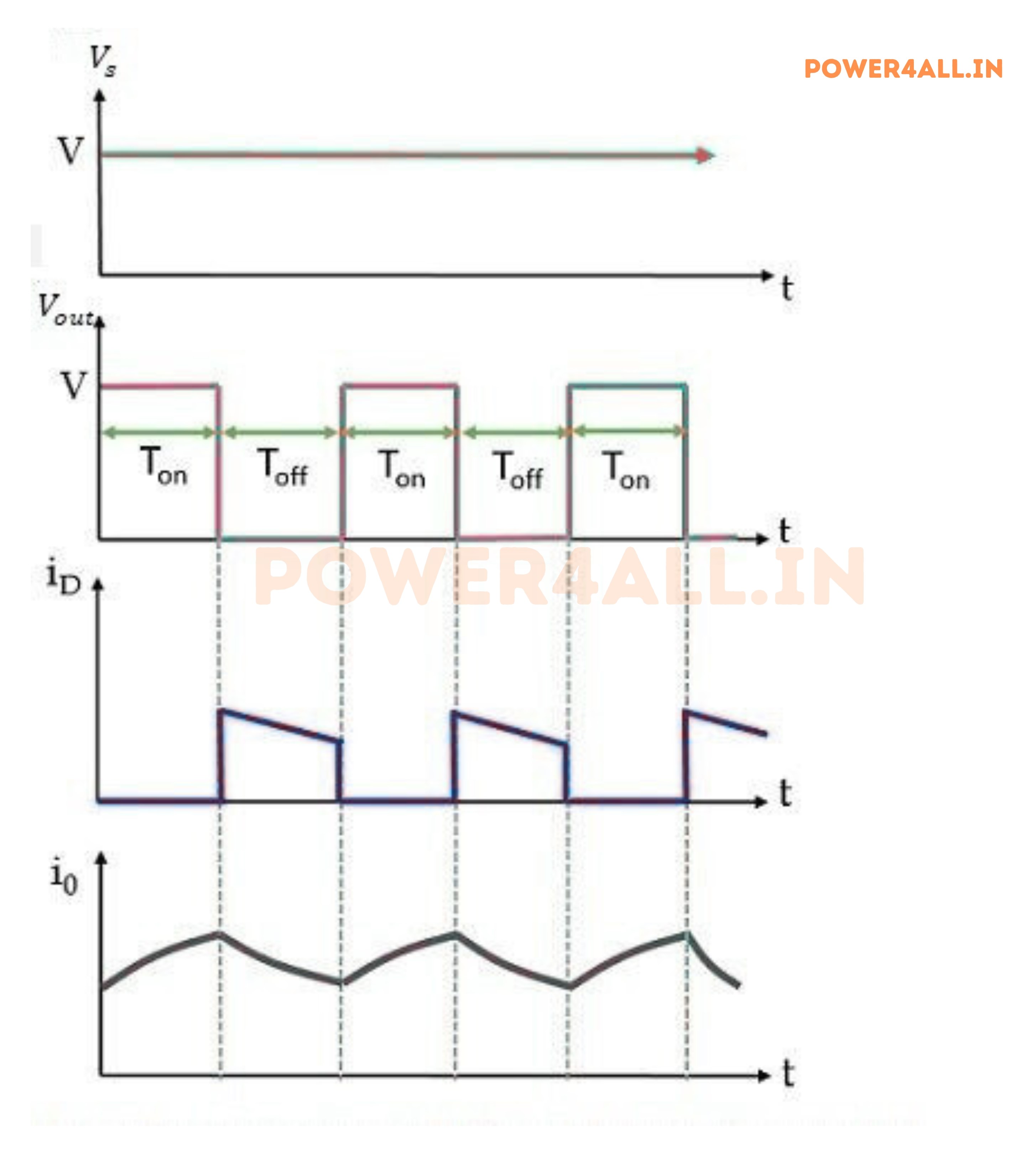
Waveform of Buck Converter
The waveform of a buck converter is characterized by its distinct voltage and current profiles during the two operational modes. The following figure illustrates the voltage and current waveforms associated with the buck converter's operation.
Advantages of Buck Converter
The buck converter offers several advantages, making it a popular choice in various applications:
- High Efficiency: Buck converters are known for their high efficiency, often exceeding 90%, which minimizes energy loss.
- Compact Size: Their compact design allows for integration into smaller devices and systems.
- Wide Input Voltage Range: Buck converters can operate over a wide range of input voltages, making them versatile.
- Low Output Ripple: They provide a stable output voltage with low ripple, ensuring reliable performance.
- Cost-Effective: Buck converters are cost-effective solutions for voltage regulation in various applications.
Disadvantages of Buck Converter
While buck converters have many advantages, they also have some disadvantages:
- Complex Control: The control circuitry can be complex, especially for high-frequency applications.
- Electromagnetic Interference (EMI): Switching action can generate EMI, requiring careful design to mitigate.
- Limited Output Voltage Range: Buck converters can only step down voltage, not step up.
- Inductor Size: The inductor size can be relatively large, affecting the overall size of the converter.
Applications of Buck Converter
Buck converters find applications in various fields, including:
- Power Supplies: Used in computer power supplies and battery chargers.
- Electric Vehicles: Employed in electric vehicle charging systems.
- Renewable Energy: Utilized in solar power systems for voltage regulation.
- Consumer Electronics: Found in smartphones, tablets, and other portable devices.
Conclusion
In conclusion, the buck converter is a highly efficient and versatile DC-DC converter that plays a crucial role in modern power electronics. Its ability to step down voltage while maintaining high efficiency makes it suitable for a wide range of applications, from consumer electronics to renewable energy systems. Understanding its working principle, advantages, and applications is essential for engineers and designers in the field of power electronics.