Complete BJT Transistor Mastery Guide
Master the fundamentals of Bipolar Junction Transistors - from basic principles and construction to advanced applications in amplification, switching, and modern electronic circuits
Complete Learning Path - BJT Fundamentals to Applications
Navigate through comprehensive coverage of BJTs from basic principles to advanced applications
What is a BJT Transistor?
A Bipolar Junction Transistor (BJT) is a three-terminal semiconductor device that can amplify signals or act as an electronic switch. It's called "bipolar" because it uses both electrons and holes (positive charge carriers) for its operation, and "junction" because it contains two p-n junctions formed by three layers of semiconductor material.
IC = β × IB
Collector current equals Current gain times Base current
Why BJTs are Essential
BJTs revolutionized electronics by providing the ability to amplify weak signals and create complex switching circuits. Before transistors, vacuum tubes performed these functions but were large, power-hungry, and unreliable. BJTs made modern electronics possible.
Signal Amplification
BJTs can amplify weak signals like audio, radio waves, or sensor outputs, making them stronger and usable for speakers, transmitters, or processing circuits.
Electronic Switching
BJTs can act as electronic switches, turning circuits on and off much faster than mechanical switches, enabling digital logic and computer operations.
Current Control
A small base current can control a much larger collector current, providing current gain (β) typically ranging from 10 to 1000 times.
Fast Response
BJTs can switch or change their output very quickly (nanoseconds), making them suitable for high-frequency applications and fast digital circuits.
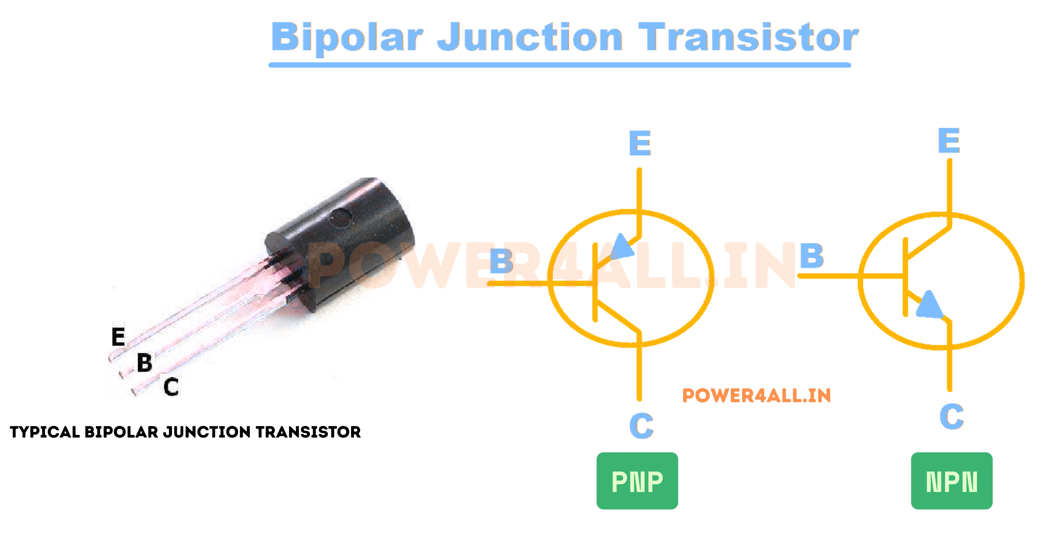
BJT Symbol and Terminals
Circuit Symbols
- NPN Symbol: Arrow pointing OUT from base (Not Pointing iN)
- PNP Symbol: Arrow pointing IN to base (Pointing iN)
- Emitter Arrow: Shows direction of conventional current
- Base: Control terminal (thin line)
- Collector: Main current collection terminal
Terminal Functions
- Emitter (E): Emits charge carriers into the base
- Base (B): Controls the current flow (very thin region)
- Collector (C): Collects charge carriers from emitter
- Current relationship: IE = IB + IC
- Typical operation: IB << IC (base current much smaller)
BJT Applications in Everyday Life
- Audio amplifiers: Amplify weak microphone signals for speakers
- Radio receivers: Amplify weak radio signals from antennas
- Digital circuits: Form logic gates in computers and microprocessors
- Power control: Switch motors, lights, and other high-power devices
- Sensors: Amplify weak signals from temperature, light, or pressure sensors
- Oscillators: Generate clock signals and carrier waves for communications
Historical Impact
The transistor was invented at Bell Labs in 1947 by John Bardeen, Walter Brattain, and William Shockley, earning them the 1956 Nobel Prize in Physics. This invention launched the electronics revolution, leading to computers, smartphones, and the digital age we live in today!
BJT Fundamentals & Physics of Operation
Understanding how BJTs work requires exploring the semiconductor physics, p-n junctions, and charge carrier movement that enables these devices to amplify and switch. This foundation is crucial for understanding BJT behavior and designing effective circuits.
Semiconductor Physics Basics
Understanding the Building Blocks of BJTs
Pure and Doped Semiconductors
BJTs are made from silicon or germanium crystals that have been "doped" with tiny amounts of other elements to create regions with different electrical properties.
| Material Type | Dopant | Charge Carriers | Characteristics |
|---|---|---|---|
| N-type | Phosphorus, Arsenic | Electrons (negative) | Extra electrons available for conduction |
| P-type | Boron, Aluminum | Holes (positive) | Missing electrons create positive holes |
| Pure Silicon | None | Very few | Poor conductor at room temperature |
Doping Concentration
- Pure silicon: 10²² atoms per cm³
- Dopant atoms: 10¹⁵ - 10¹⁹ atoms per cm³
- Ratio: Only 1 in 1 million to 1 in 1000 atoms are dopants
- Effect: Dramatically changes electrical properties
P-N Junction Behavior
Junction Formation
When P-type and N-type materials are joined, electrons and holes diffuse across the boundary, creating a depletion region with an internal electric field.
Forward Bias (Junction ON)
- P-side connected to positive voltage
- N-side connected to negative voltage
- External field opposes internal field
- Current flows easily (low resistance)
- Voltage drop: ~0.7V for silicon, ~0.3V for germanium
Reverse Bias (Junction OFF)
- P-side connected to negative voltage
- N-side connected to positive voltage
- External field reinforces internal field
- Very little current flows (high resistance)
- Depletion region widens
I = Is(e^(qV/kT) - 1)
Diode equation governs p-n junction current
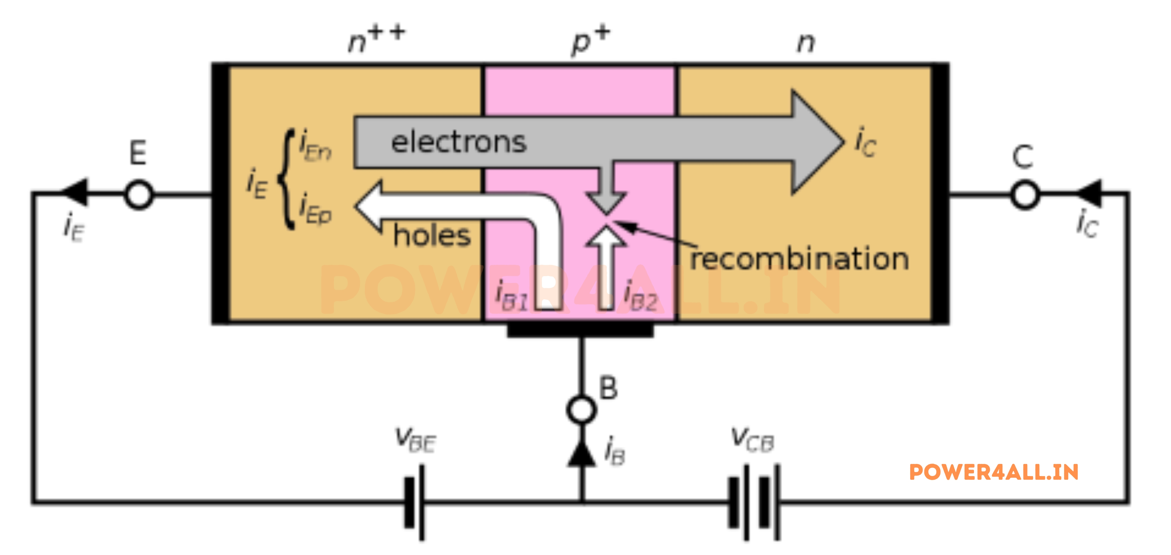
BJT Operation Principle
Current Control Mechanism
How a small base current controls large collector current
Base Region Design
Why the base must be very thin
Critical Design Requirements
- Thin base: Typically 1-10 micrometers thick
- Light doping: Low concentration of charge carriers
- High recombination rate: Would reduce efficiency if too thick
- Transit time: Carriers must cross quickly
Base Thickness Effect
- Too thick: Carriers recombine before reaching collector
- Too thin: Difficult to make reliable contacts
- Just right: 95%+ of carriers reach collector
- Modern BJTs: Base can be < 1 micrometer
Key Parameters
Important BJT specifications and relationships
Current Gain (β or hFE)
β = IC / IB
Current gain relates collector to base current
Alpha (α)
α = IC / IE
Current transfer ratio (always < 1)
Relationship Between α and β
β = α / (1 - α)
Connection between the two gain parameters
Temperature Effects on BJT Operation
How Temperature Affects BJT Performance
Temperature has significant effects on BJT behavior, which must be considered in circuit design for reliable operation across temperature ranges.
| Parameter | Temperature Effect | Typical Change | Design Impact |
|---|---|---|---|
| Base-Emitter Voltage (VBE) | Decreases with temperature | -2mV/°C | Bias point shifts |
| Current Gain (β) | Increases with temperature | +0.5%/°C to +1%/°C | Gain variation affects amplification |
| Leakage Current (ICO) | Doubles every 10°C | ×2 per 10°C | Significant at high temperatures |
| Breakdown Voltages | Slight temperature dependence | ±0.1%/°C | Usually negligible |
Thermal Runaway
In power BJTs, increased temperature causes increased current, which causes more heating, leading to thermal runaway and device destruction. Proper heat sinking and current limiting are essential for power applications.
Types of BJT: NPN and PNP Transistors
BJTs come in two complementary types: NPN and PNP. While they operate on the same basic principles, their internal structure and current flow directions are opposite. Understanding both types is essential for designing circuits and choosing the right transistor for specific applications.
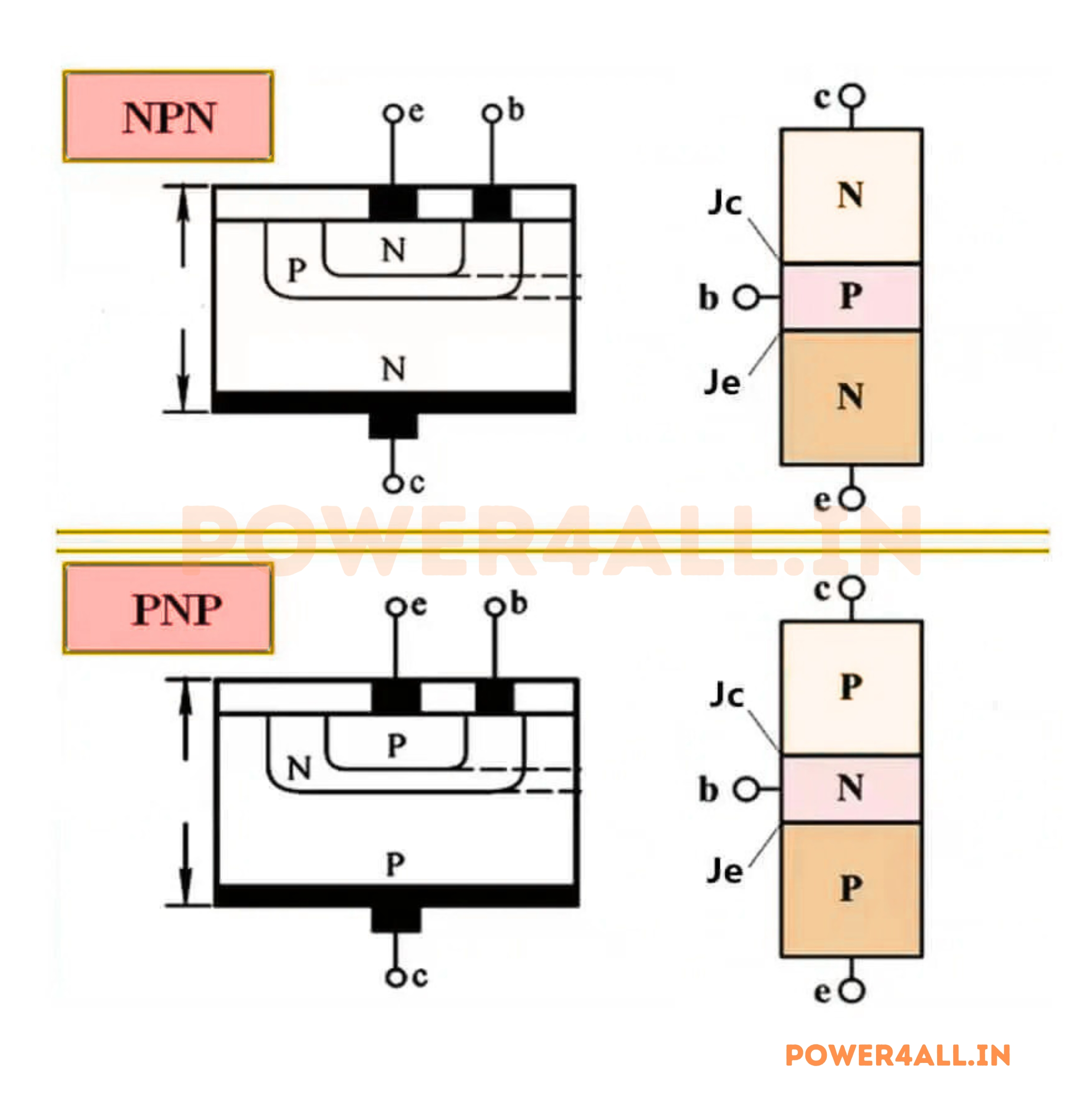
NPN Transistors
NPN Structure & Operation
N-P-N layered semiconductor structure
Physical Structure
- Emitter: N-type (heavily doped with electrons)
- Base: P-type (thin, lightly doped)
- Collector: N-type (moderately doped)
- Symbol: Arrow points OUT from base (Not Pointing iN)
Current Flow
- Electrons flow: Emitter → Base → Collector
- Conventional current: Collector → Emitter
- Base current: Into the base terminal
- Turn-on: Base positive relative to emitter
NPN Biasing
- VBE ≈ +0.7V: Forward bias base-emitter junction
- VCE > VBE: Reverse bias collector-base junction
- IB > 0: Base current flows into base
- IC = β × IB: Collector current controlled by base
NPN Advantages
Why NPN is more common in circuits
Performance Benefits
- Higher mobility: Electrons move faster than holes
- Better frequency response: Faster switching speeds
- Higher current capability: Can handle more current
- Lower noise: Better signal-to-noise ratio
- More available: Wider selection of NPN devices
Common Applications
- Amplifiers: Audio, RF, and general purpose
- Switches: Digital logic and power control
- Oscillators: Clock generation and RF sources
- Voltage regulators: Power supply control
PNP Transistors
PNP Structure & Operation
P-N-P layered semiconductor structure
Physical Structure
- Emitter: P-type (heavily doped with holes)
- Base: N-type (thin, lightly doped)
- Collector: P-type (moderately doped)
- Symbol: Arrow points INTO base (Pointing iN)
Current Flow
- Holes flow: Emitter → Base → Collector
- Conventional current: Emitter → Collector
- Base current: Out of the base terminal
- Turn-on: Base negative relative to emitter
PNP Biasing
- VEB ≈ +0.7V: Forward bias emitter-base junction
- VEC > VEB: Reverse bias collector-base junction
- IB < 0: Base current flows out of base
- IC = β × IB: Same current gain relationship
PNP Applications
Where PNP transistors excel
Specific Advantages
- High-side switching: Control loads connected to ground
- Complementary pairs: Work with NPN for push-pull amplifiers
- Current sourcing: Provide current to loads
- Voltage regulation: High-side control applications
Common Uses
- Current sources: Constant current supplies
- High-side switches: Control power to circuits
- Complementary amplifiers: Class B push-pull stages
- Level shifters: Interface different voltage levels
NPN vs PNP Comparison
| Characteristic | NPN Transistor | PNP Transistor | Comments |
|---|---|---|---|
| Majority Carriers | Electrons | Holes | Determines speed and performance |
| Base Current Direction | Into base | Out of base | Affects circuit design |
| Turn-on Voltage | VBE = +0.7V | VEB = +0.7V | Base-emitter junction voltage |
| Switching Speed | Faster | Slower | Electron mobility > hole mobility |
| Cost/Availability | Lower cost, more options | Higher cost, fewer options | Manufacturing preferences |
| Power Handling | Generally higher | Generally lower | Thermal and electrical limits |
Complementary Pair Applications
Using NPN and PNP Together for Enhanced Performance
Many advanced circuits use both NPN and PNP transistors together to create complementary pairs that provide superior performance compared to single-type designs.
Push-Pull Output Stages
Class B Amplifiers
NPN handles positive half-cycles, PNP handles negative half-cycles, providing efficient power amplification with low quiescent current.
Totem Pole Outputs
Digital circuits use complementary pairs for fast switching with strong pull-up and pull-down capability.
Current Mirrors
Precision current sources using matched NPN/PNP pairs for stable, temperature-compensated operation.
Differential Pairs
Balanced amplifiers with excellent common-mode rejection and low offset voltage drift.
Common Complementary Pairs
- 2N3904/2N3906: General purpose small signal
- 2N2222/2N2907: Popular general purpose pair
- BD139/BD140: Medium power complementary pair
- 2N3055/2N2955: High power audio applications
- TIP31/TIP32: Medium power switching and amplification
Design Tip
When choosing between NPN and PNP, consider: NPN for general applications requiring speed and performance, PNP for high-side switching and current sourcing, and complementary pairs for balanced, high-performance circuits. Most beginners should start with NPN transistors due to their availability and ease of use.
BJT Construction & Physical Structure
The physical construction of a BJT determines its electrical characteristics, power handling capability, frequency response, and reliability. Understanding how BJTs are made and packaged helps in selecting the right device and understanding its limitations and optimal operating conditions.
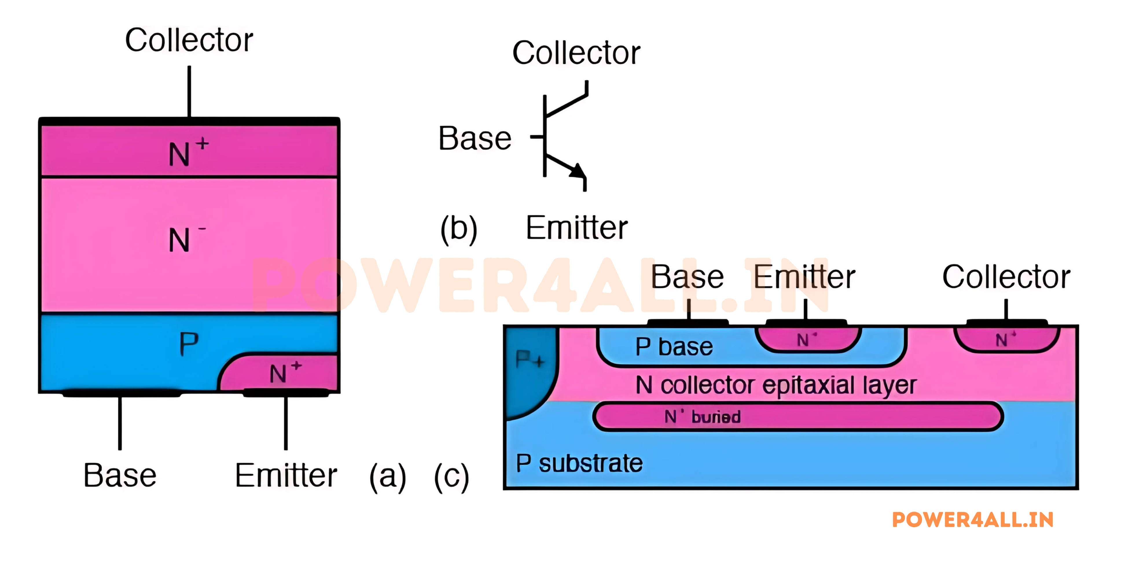
Manufacturing Process
Silicon Wafer Fabrication
BJTs start as pure silicon crystals grown into large cylindrical ingots, then sliced into thin wafers. These wafers undergo multiple processing steps to create thousands of transistors simultaneously.
Wafer Specifications
- Diameter: 200mm (8") or 300mm (12") typical
- Thickness: 0.7mm to 1.0mm
- Crystal orientation: <100> for best electrical properties
- Purity: 99.9999999% pure silicon (9N purity)
- Devices per wafer: Thousands to millions
Doping and Junction Formation
Diffusion Process
Creating the three-layer NPN or PNP structure
Step-by-Step Doping
Doping Concentrations
- Emitter: 10¹⁹ atoms/cm³ (heavily doped)
- Base: 10¹⁶ atoms/cm³ (lightly doped)
- Collector: 10¹⁵ atoms/cm³ (moderately doped)
- Substrate: 10¹⁴ atoms/cm³ (lightly doped)
Ion Implantation
Modern precision doping technique
Process Advantages
- Precise control: Exact dopant concentration and depth
- Uniform distribution: Consistent across wafer
- Low temperature: Doesn't disturb previous layers
- Selective doping: Only where photoresist allows
- Reproducible: Consistent device parameters
Implantation Parameters
- Ion energy: 10keV to 200keV typical
- Dose: 10¹² to 10¹⁶ ions/cm²
- Beam current: Microamps to milliamps
- Vacuum level: 10⁻⁶ torr or better
Photolithography
Pattern definition for device structures
Process Steps
Package Types and Thermal Considerations
From Die to Finished Package - Protection and Heat Management
Common Package Types
| Package Type | Power Rating | Thermal Resistance | Applications | Mounting |
|---|---|---|---|---|
| TO-92 | 0.5W - 1W | 200°C/W | Small signal, low power | Through hole, 3 leads |
| SOT-23 | 0.2W - 0.5W | 300°C/W | Surface mount, compact | SMD, 3 terminals |
| TO-220 | 20W - 150W | 5°C/W to case | Power applications | Through hole, heat sink tab |
| TO-3 | 100W - 300W | 1.5°C/W to case | High power audio, linear | Metal can, bolt mounting |
| SOT-89 | 1W - 2W | 50°C/W | SMD medium power | Surface mount with tab |
Thermal Management
Heat Sinks
Metal heat sinks increase surface area for heat dissipation. Size and design depend on power dissipation and ambient temperature.
Forced Air Cooling
Fans improve heat sink effectiveness by 3-10x, enabling higher power operation in smaller packages.
Thermal Interface
Thermal compound or pads improve heat transfer between device case and heat sink, reducing thermal resistance.
PCB Thermal Design
Copper planes, thermal vias, and component placement help spread and dissipate heat in surface mount applications.
TJ = TA + (θJA × PD)
Junction temperature = Ambient + (Thermal resistance × Power dissipated)
Thermal Calculation Example
TO-220 BJT dissipating 10W in 25°C ambient:
- Without heat sink: θJA = 62°C/W → TJ = 25°C + (62 × 10) = 645°C (destroyed!)
- With heat sink: θJA = 8°C/W → TJ = 25°C + (8 × 10) = 105°C (safe operation)
- Maximum rating: Usually 150°C junction temperature
- Design margin: Keep TJ < 125°C for reliability
BJT Operating Regions & Modes
Understanding the different operating regions of a BJT is crucial for predicting its behavior in circuits. Each region has distinct characteristics and applications, from linear amplification to digital switching. The bias conditions of the two junctions determine which region the transistor operates in.
Active Region (Linear Operation)
Active Region Characteristics
The amplification region for linear circuits
Bias Conditions
- Base-Emitter: Forward biased (VBE ≈ 0.7V)
- Collector-Base: Reverse biased (VCB > 0)
- Collector-Emitter: VCE > VBE (typically > 0.2V)
- Base current: Controls collector current
IC = β × IB
Linear relationship in active region
Key Properties
- Linear amplification: Output proportional to input
- High input impedance: Base circuit doesn't load signal
- Current gain: β typically 50-500
- Variable VCE: Depends on load and bias
Active Region Applications
Where linear amplification is needed
Amplifier Circuits
- Audio amplifiers: Music and voice amplification
- RF amplifiers: Radio frequency signal boosting
- Operational amplifiers: Building blocks for analog circuits
- Buffer amplifiers: Impedance isolation and drive capability
- Differential amplifiers: Precise signal comparison
Signal Processing
- Filters: Active filters for frequency selection
- Oscillators: Signal generation for clocks and carriers
- Mixers: Frequency conversion in communications
- Detectors: Signal demodulation and detection
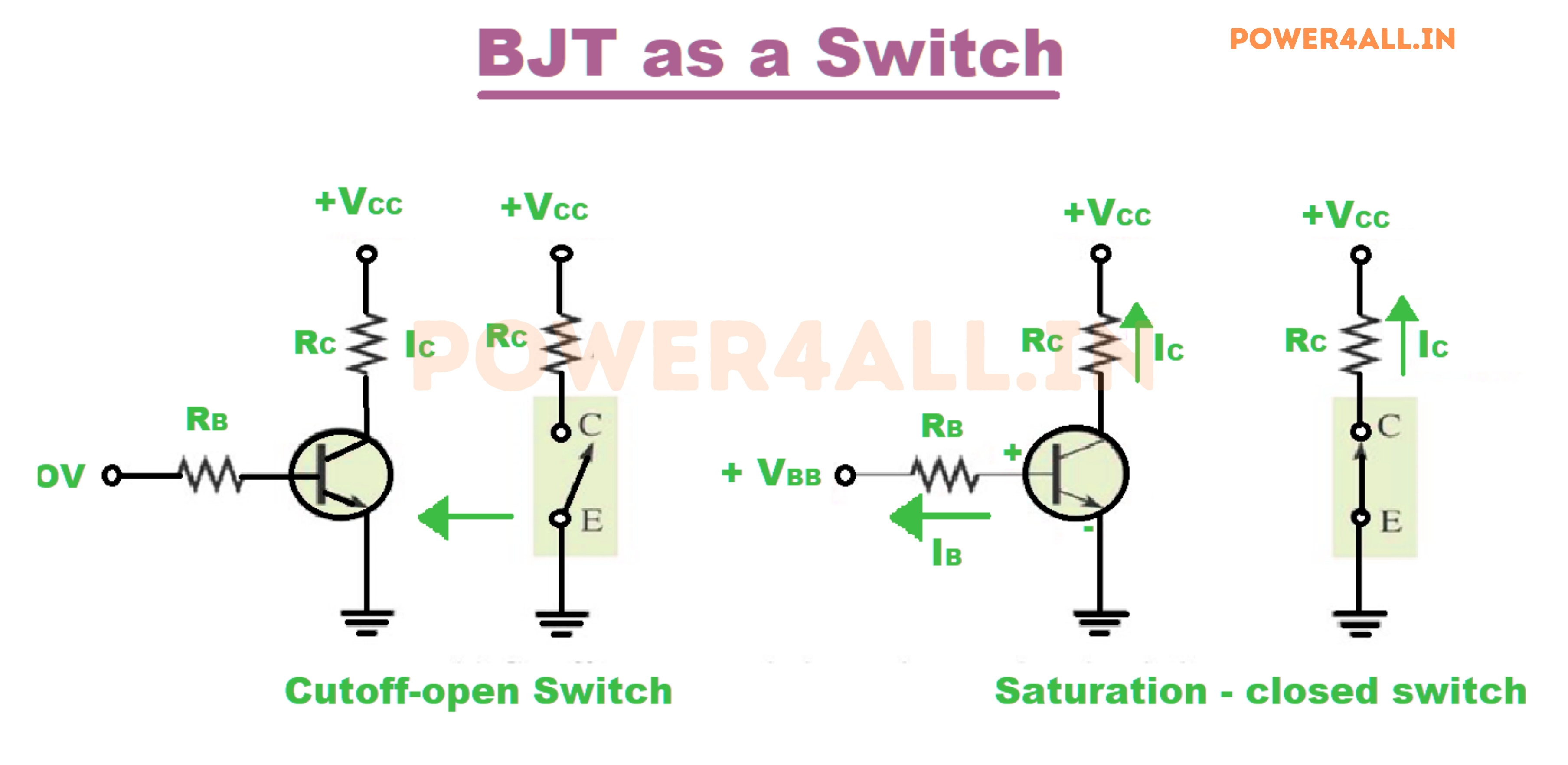
Saturation Region (Switch ON)
Saturation Characteristics
In saturation, the BJT acts like a closed switch with minimal voltage drop between collector and emitter. Both junctions are forward biased, and the transistor is fully turned on.
Bias Conditions
- Base-Emitter: Forward biased (VBE ≈ 0.7V)
- Collector-Base: Forward biased (VCB ≈ 0.5V)
- VCE(sat): Very low (0.1V - 0.3V typical)
- Base overdrive: IB >> IC/β
Saturation Design Example
Switch 1A load with 5V supply:
- Required IC: 1A
- Transistor β: 100 minimum
- Base current needed: IB > 1A/100 = 10mA
- Design base current: 20mA (2× overdrive)
- VCE(sat): ~0.2V (very low resistance)
- Power in switch: 1A × 0.2V = 0.2W
Digital Logic
Saturation represents logic "1" or "ON" state in digital circuits, with minimum voltage drop for efficient switching.
Power Switching
Low VCE(sat) minimizes power dissipation when controlling motors, relays, and LED drivers.
Storage Time
Excess base charge must be removed before transistor can turn off, causing switching delay.
Safe Operation
Proper base drive ensures reliable saturation even with temperature and β variations.
Cutoff Region (Switch OFF)
Cutoff Characteristics
The "OFF" state with minimal current flow
Bias Conditions
- Base-Emitter: Reverse biased (VBE < 0.5V)
- Collector-Base: Reverse biased (VCB > 0)
- Base current: IB ≈ 0 (or negative)
- Collector current: IC ≈ ICEO (leakage only)
Leakage Currents
- ICEO: Collector-emitter leakage (base open)
- ICBO: Collector-base leakage (emitter open)
- Temperature effect: Doubles every 10°C
- Practical impact: Usually negligible at room temperature
Cutoff Applications
High efficiency switching and digital logic
Digital Applications
- Logic gates: Represents logic "0" or "OFF"
- Memory circuits: Data storage in bistable circuits
- Counters: Digital counting and timing circuits
- Microprocessors: Billions of switching transistors
Power Control
- Power switches: Turn off high-power loads
- Battery conservation: Minimize standby current
- Safety circuits: Emergency shutdown capability
- Sleep modes: Low-power standby operation
Region Comparison and Transition
| Parameter | Cutoff | Active | Saturation | Units |
|---|---|---|---|---|
| VBE | < 0.5 | ≈ 0.7 | ≈ 0.8 | Volts |
| VCE | ≈ VCC | Variable | < 0.3 | Volts |
| IC | ≈ 0 | β × IB | Limited by circuit | Amperes |
| Power Dissipation | Very low | Medium to high | Low | Watts |
| Applications | Switch OFF, Logic 0 | Amplifiers | Switch ON, Logic 1 | - |
Power Dissipation Warning
Maximum power dissipation occurs in the active region where both VCE and IC are significant (P = VCE × IC). Switching applications are more efficient because power is low in both cutoff (IC ≈ 0) and saturation (VCE ≈ 0). Always check that power dissipation doesn't exceed the device rating, especially in linear applications.
BJT Configurations: Common Emitter, Base, and Collector
BJTs can be connected in three basic configurations, each with unique input/output characteristics, gain properties, and applications. Understanding these configurations is essential for designing amplifiers, buffers, and other analog circuits with optimal performance for specific requirements.
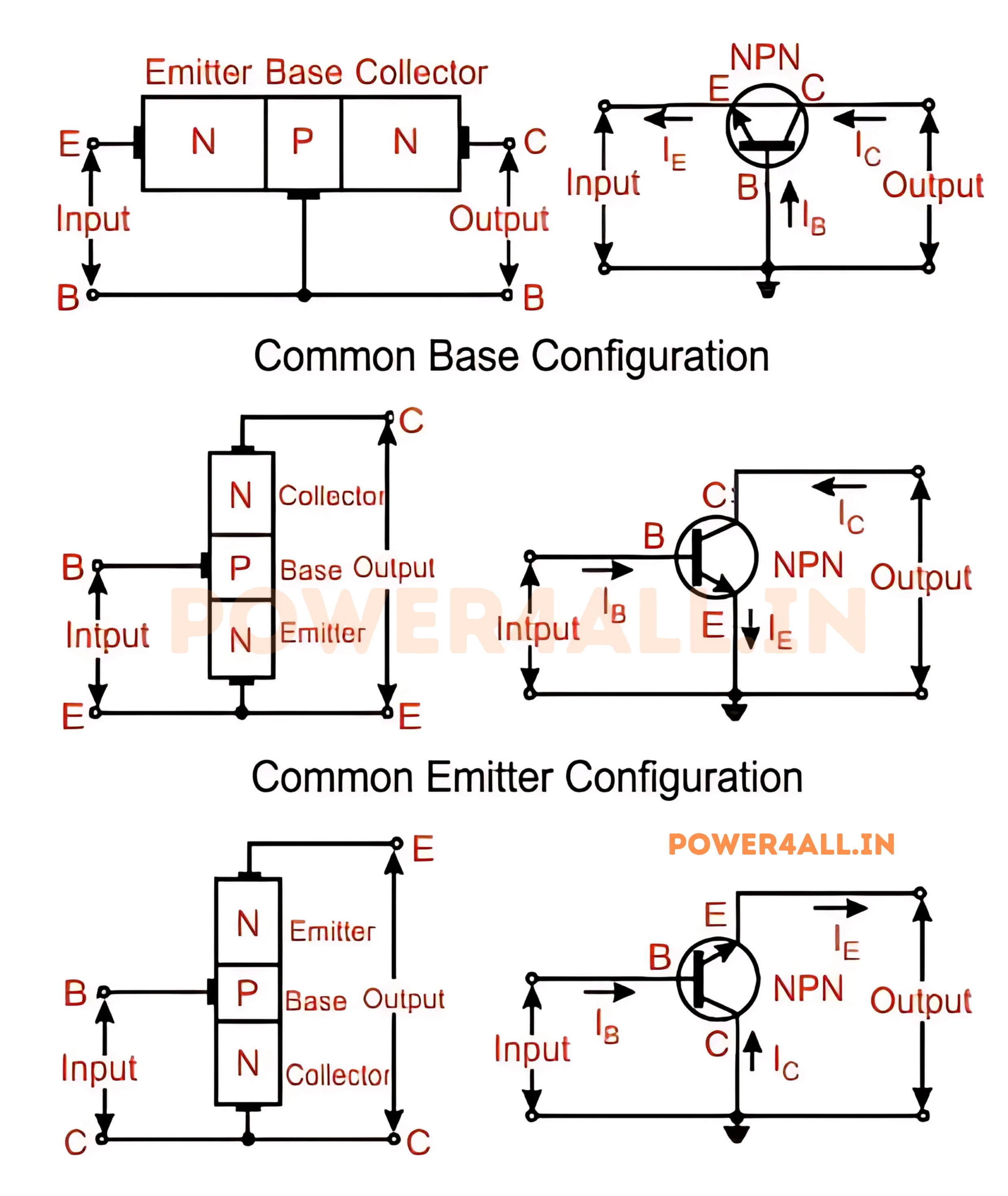
Common Emitter (CE) Configuration
CE Configuration Properties
Most popular configuration for voltage amplification
Connection Details
- Input: Between base and emitter
- Output: Between collector and emitter
- Common terminal: Emitter (usually grounded)
- Signal inversion: 180° phase shift
Key Characteristics
- Voltage gain: High (50-500 typical)
- Current gain: High (β = 50-300)
- Power gain: Very high (Av × Ai)
- Input impedance: Medium (1kΩ-10kΩ)
- Output impedance: High (10kΩ-100kΩ)
Av = -RC / re
Voltage gain for CE amplifier
CE Applications
Where high gain and signal inversion are needed
Amplifier Applications
- Audio preamplifiers: Boost microphone signals
- RF amplifiers: Radio frequency signal amplification
- Instrumentation: Sensor signal conditioning
- Communication: IF and baseband amplifiers
- Test equipment: Oscilloscope front ends
Circuit Examples
- Single-stage amplifier: Basic voltage amplification
- Multi-stage cascades: Higher overall gain
- Darlington pairs: Very high current gain
- Differential amplifiers: Balanced amplification
CE Design Example
Audio amplifier stage:
- Voltage gain: 40dB (100×)
- Input signal: 10mV RMS
- Output signal: 1V RMS
- Phase shift: 180° inversion
- Bandwidth: 20Hz - 20kHz
Common Base (CB) Configuration
CB Configuration Properties
High frequency performance with current-to-voltage conversion
Connection Details
- Input: Between emitter and base
- Output: Between collector and base
- Common terminal: Base (AC grounded)
- Phase relationship: No inversion (0°)
Key Characteristics
- Voltage gain: High (similar to CE)
- Current gain: Less than unity (α < 1)
- Power gain: Medium
- Input impedance: Very low (10Ω-100Ω)
- Output impedance: Very high (100kΩ+)
- Frequency response: Excellent high-frequency
α = IC / IE ≈ 0.98-0.995
Current transfer ratio in CB
CB Applications
High-frequency and current-to-voltage conversion
RF Applications
- RF amplifiers: VHF/UHF frequency ranges
- Oscillators: High-frequency signal generation
- Mixers: Frequency conversion circuits
- Buffer amplifiers: Isolation between stages
- Cascode amplifiers: Combined with CE for high gain
Special Characteristics
- Low input impedance: Good for current sources
- High frequency cutoff: fα >> fβ
- No Miller effect: Better high-frequency response
- Voltage-to-current conversion: Transconductance amplifier
CB Frequency Advantage
- Unity gain frequency: fT = 300MHz (example)
- CE cutoff: fβ = fT/β = 3MHz (β=100)
- CB cutoff: fα ≈ fT = 300MHz
- Performance: 100× better high-frequency response
Common Collector (CC) Configuration
CC Configuration Properties
Unity voltage gain with high current gain - "Emitter Follower"
Connection Details
- Input: Between base and collector
- Output: Between emitter and collector
- Common terminal: Collector (usually at VCC)
- Phase relationship: No inversion (0°)
- Alternative name: Emitter follower
Key Characteristics
- Voltage gain: ≈ 1 (0.95-0.99 typical)
- Current gain: High (β + 1)
- Power gain: Medium (equal to current gain)
- Input impedance: Very high (>100kΩ)
- Output impedance: Very low (<100Ω)
Av ≈ 1
Voltage follows input (emitter follower)
CC Applications
Buffer amplifiers and impedance matching
Buffer Applications
- Impedance isolation: Connect high-Z source to low-Z load
- Current boosting: Provide higher drive current
- Voltage following: Output tracks input voltage
- Power amplification: Increase signal power capability
- Line driving: Drive long cables or transmission lines
Practical Examples
- Op-amp output buffers: Increase current drive capability
- ADC input buffers: Isolate sensor from ADC loading
- Crystal oscillator buffers: Prevent loading of oscillator
- Audio line drivers: Drive headphones or speakers
Buffer Design Example
Sensor buffer for 0-5V signal:
- Input impedance: >1MΩ (doesn't load sensor)
- Output impedance: <50Ω (drives cables well)
- Voltage gain: 0.99 (minimal loss)
- Current gain: 200+ (high drive capability)
- Power gain: 200× improvement
Configuration Comparison
| Parameter | Common Emitter (CE) | Common Base (CB) | Common Collector (CC) |
|---|---|---|---|
| Voltage Gain | High (50-500) | High (50-500) | ≈ 1 |
| Current Gain | Medium (β) | <1 (α) | High (β + 1) |
| Power Gain | Very High | Medium | Medium |
| Input Impedance | Medium (1-10kΩ) | Low (10-100Ω) | Very High (>100kΩ) |
| Output Impedance | High (10-100kΩ) | Very High (>100kΩ) | Low (<100Ω) |
| Phase Shift | 180° | 0° | 0° |
| Best Use | General amplification | High frequency amplification | Buffer and isolation |
BJT Biasing Techniques & Circuits
Proper biasing is crucial for BJT operation, setting the correct DC operating point (Q-point) to ensure the transistor operates in the desired region under all conditions. Good biasing provides temperature stability and consistent performance across component variations.
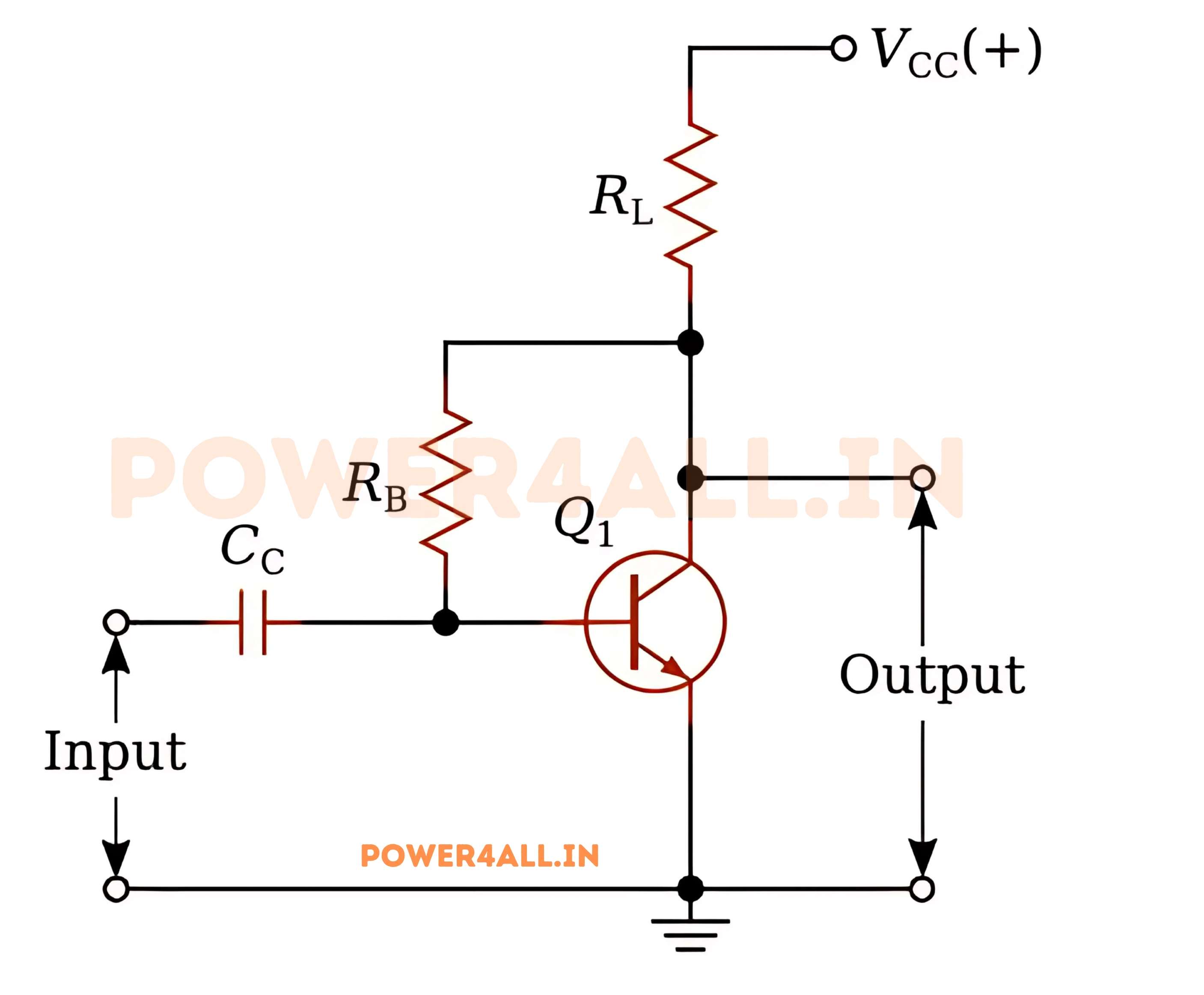
Fixed Bias (Base Bias)
Simple Fixed Bias Circuit
Simplest but least stable biasing method
Circuit Description
- Base resistor: RB connected from VCC to base
- Collector resistor: RC from VCC to collector
- Base current: Set by RB and VCC
- Operating point: Depends heavily on β
IB = (VCC - VBE) / RB
Base current calculation
IC = β × IB
Collector current (β dependent)
Fixed Bias Problems
Why fixed bias is rarely used in practice
Major Issues
- β dependence: Operating point varies with transistor β
- Temperature sensitivity: Q-point shifts with temperature
- Component tolerance: Sensitive to resistor variations
- Thermal runaway: Possible in power applications
- Manufacturing variations: Inconsistent performance
β Variation Example
Same circuit with different transistors:
- Transistor A (β=100): IC = 2mA, VCE = 8V
- Transistor B (β=200): IC = 4mA, VCE = 4V
- Transistor C (β=300): IC = 6mA, VCE = 0V (saturated!)
- Problem: Same circuit, drastically different operation
Voltage Divider Bias
Most Popular Biasing Method
Voltage divider bias uses two resistors to create a stable base voltage that's relatively independent of β variations. This makes it the most widely used biasing technique.
Circuit Components
- R1: Upper voltage divider resistor
- R2: Lower voltage divider resistor
- RC: Collector load resistor
- RE: Emitter resistor (provides negative feedback)
- CE: Emitter bypass capacitor (AC applications)
VB = VCC × R2/(R1 + R2)
Base voltage from voltage divider
VE = VB - VBE
Emitter voltage
IE ≈ IC = VE / RE
Emitter/collector current
Design Rules for Voltage Divider Bias
Step-by-Step Design Process and Guidelines
Design Guidelines
Complete Design Example
Design specifications: VCC = 12V, IC = 2mA, VCE = 6V, β = 100
Other Biasing Methods
Emitter Feedback Bias
Self-adjusting bias with emitter resistor
Operation Principle
- Base resistor: Connected from VCC to base
- Emitter resistor: Provides negative feedback
- Self-regulation: Increased IC causes increased VE
- Automatic correction: Higher VE reduces VBE and IC
Feedback Action
- IC increases → VE increases → VBE decreases → IB decreases → IC decreases
- This negative feedback stabilizes the operating point
- Much better than fixed bias, simpler than voltage divider
Dual Supply Bias
Using positive and negative supplies
Advantages
- Zero input offset: Input can be AC coupled through ground
- Maximum swing: Output can swing both directions
- Excellent stability: Base at ground potential
- Simple design: Fewer bias components needed
Typical Configuration
- Supplies: +12V and -12V
- Base bias: Connected to ground through resistor
- Emitter: Connected to -VEE through resistor
- Collector: Connected to +VCC through load
- Result: Stable, symmetric operation
Active Bias Circuits
Using current sources and mirrors for precision bias
Current Source Biasing
- Constant current: Active device provides stable IC
- Temperature compensation: Can include temp compensation
- High performance: Used in IC design
- Complexity: Requires more components
Current Mirror Biasing
- Reference current: One transistor sets reference
- Mirrored current: Other transistors mirror this current
- Tracking: All bias currents track together
- IC applications: Standard in integrated circuits
Biasing Best Practices
- Use voltage divider bias for most discrete circuit applications
- Include emitter degeneration (RE) for stability
- Design for worst-case β variations (2:1 or 3:1 range)
- Consider temperature effects in critical applications
- Use bypass capacitors in AC amplifiers to maintain AC gain
- Verify operation with simulation before building
BJT Characteristics & Key Parameters
Understanding BJT characteristics and parameters is essential for proper circuit design and analysis. These specifications define the limits, performance, and behavior of transistors under various operating conditions, helping engineers select the right device and predict circuit performance.
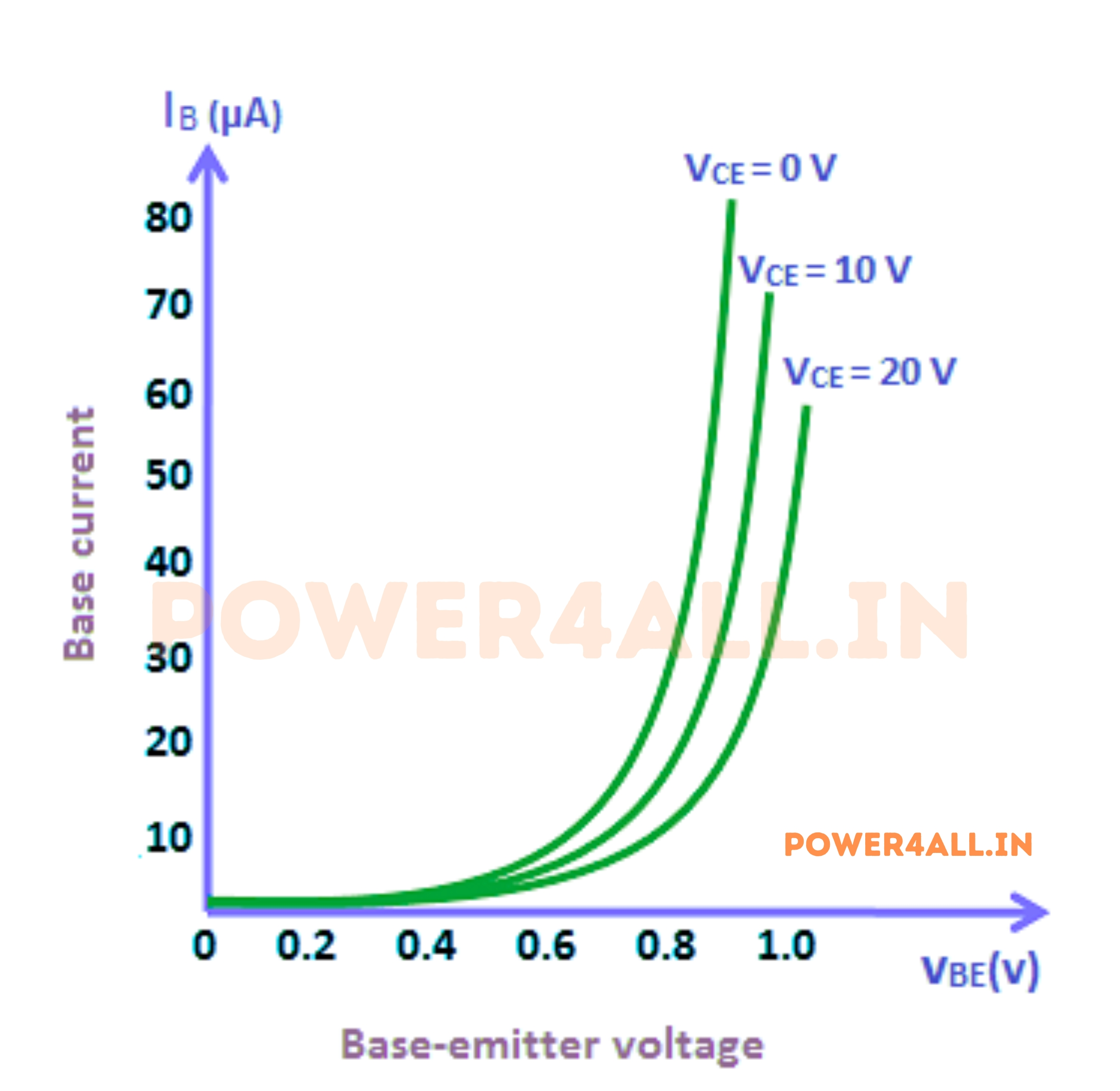
Input Characteristics
IB vs VBE Characteristics
Base current vs base-emitter voltage relationship
Key Features
- Diode-like curve: Exponential relationship similar to p-n junction
- Turn-on voltage: ~0.6-0.7V for silicon BJTs
- Temperature coefficient: -2mV/°C typical
- Current increases rapidly: Above turn-on voltage
- VCE effect: Slight dependence on collector-emitter voltage
IB = IS(e^(VBE/VT) - 1)
Exponential relationship (Shockley equation)
Practical Input Characteristics
- At VBE = 0.6V: IB ≈ 1µA
- At VBE = 0.65V: IB ≈ 10µA
- At VBE = 0.7V: IB ≈ 100µA
- Small voltage change: Large current change
- Design implication: Use current sources, not voltage sources
Input Resistance (rin)
Dynamic resistance of base-emitter junction
rin = ΔVBE / ΔIB
Dynamic input resistance
Typical Values
- Small signal BJTs: 1kΩ - 10kΩ
- Power BJTs: 100Ω - 1kΩ
- High β transistors: Higher input resistance
- Temperature effect: Increases with temperature
Input Resistance Calculation
For common emitter configuration:
- rin(base) = VT/IB: Intrinsic base resistance
- rin(total) = β × re: Including emitter resistance
- re = VT/IE: Emitter dynamic resistance
- At IE = 1mA: re = 26mV/1mA = 26Ω
- If β = 100: rin(total) = 100 × 26Ω = 2.6kΩ
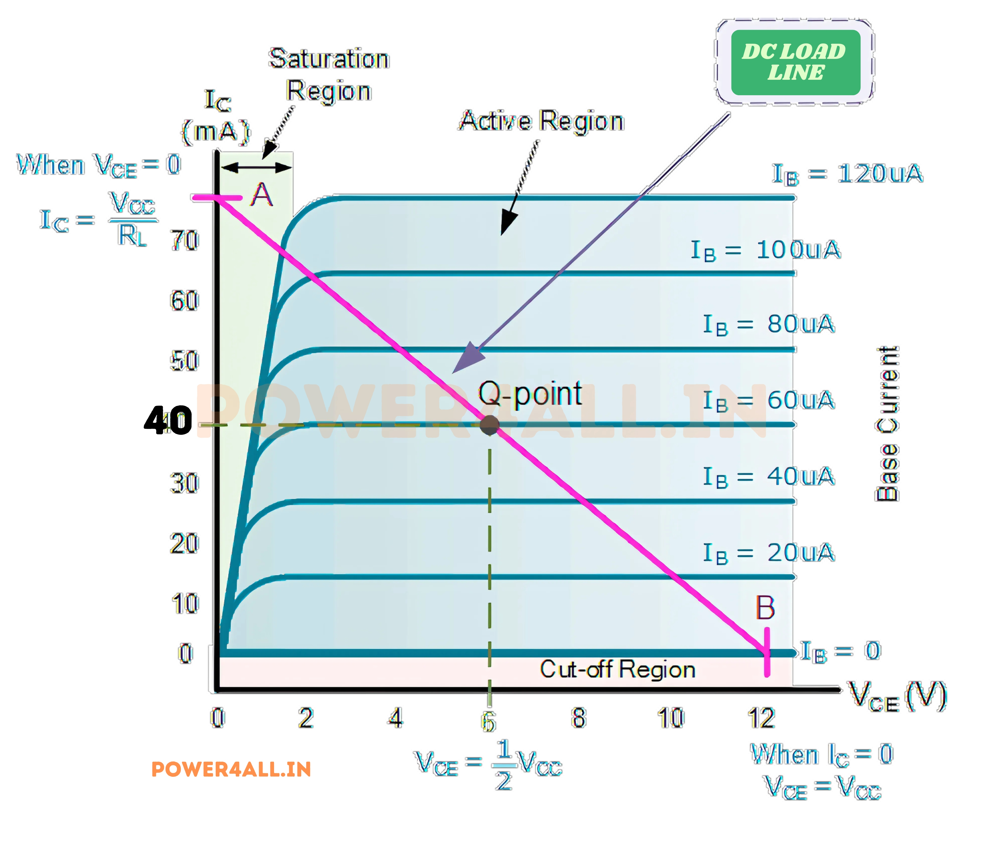
Output Characteristics
IC vs VCE Family of Curves
The output characteristics show how collector current varies with collector-emitter voltage for different base current values. These curves define the operating regions and limits.
Curve Regions
- Active region: Flat portion, constant IC for given IB
- Saturation region: Low VCE, IC limited by external circuit
- Cutoff region: IB = 0, only leakage current flows
- Breakdown region: High VCE causes avalanche breakdown
Reading Output Characteristics
From typical IC vs VCE curves:
- Load line: Shows possible operating points
- Q-point: Intersection of load line and IB curve
- β extraction: β = IC/IB at any point in active region
- Early voltage: Extrapolation of active region lines
- Output resistance: Slope of curves in active region
Key BJT Parameters
| Parameter | Symbol | Typical Range | Description | Test Conditions |
|---|---|---|---|---|
| DC Current Gain | β, hFE | 50 - 800 | Ratio of collector to base current | Specified IC, VCE |
| Collector Current | IC(max) | 10mA - 100A | Maximum continuous collector current | With adequate heat sinking |
| Collector-Emitter Voltage | VCEO | 5V - 1500V | Maximum VCE with base open | Base open circuit |
| Collector-Base Voltage | VCBO | 7V - 2000V | Maximum VCB with emitter open | Emitter open circuit |
| Emitter-Base Voltage | VEBO | 5V - 10V | Maximum reverse VEB | Collector open circuit |
| Power Dissipation | PD(max) | 0.1W - 1000W | Maximum power dissipation | At specified case temperature |
| Junction Temperature | TJ(max) | 125°C - 200°C | Maximum junction temperature | For reliable operation |
| Transition Frequency | fT | 1MHz - 100GHz | Unity gain frequency | Small signal conditions |
Frequency Response Parameters
High-Frequency Performance and Limitations
Key Frequency Parameters
Transition Frequency (fT)
Unity gain frequency - where current gain = 1
fT = β × fβ
Gain-bandwidth product
Significance
- Performance indicator: Higher fT = better high-frequency performance
- Design limitation: Gain × bandwidth ≤ fT
- Technology indicator: Shows process capabilities
- Application guide: Choose fT >> operating frequency
fT Application Example
- Transistor fT: 300MHz
- Desired gain: 100× (40dB)
- Maximum frequency: 300MHz/100 = 3MHz
- Design rule: Use below 1MHz for margin
Switching Times
Speed limitations in digital applications
Switching Parameters
- ton (turn-on delay): Base current applied to IC starts rising
- tr (rise time): IC rises from 10% to 90%
- ts (storage time): Delay when turning off from saturation
- tf (fall time): IC falls from 90% to 10%
Typical Switching Times
- Small signal BJT: ton=2ns, tr=3ns, ts=20ns, tf=5ns
- Power BJT: ton=50ns, tr=100ns, ts=500ns, tf=200ns
- Limitation: Storage time dominates in saturated switching
- Improvement: Avoid deep saturation for speed
Capacitive Effects
BJT frequency limitations come from internal capacitances between the junctions and terminals.
| Capacitance | Location | Typical Value | Effect on Performance |
|---|---|---|---|
| Cje (input capacitance) | Base-emitter junction | 1-100 pF | Limits input frequency response |
| Cjc (feedback capacitance) | Collector-base junction | 0.1-10 pF | Miller effect, reduces gain at high frequency |
| Ccs (output capacitance) | Collector-substrate | 0.1-5 pF | Affects output loading |
Practical BJT Applications
BJTs find applications in virtually every area of electronics, from simple switching circuits to complex analog and digital systems. Understanding these applications helps in selecting appropriate transistors and designing effective circuits for specific purposes.
Amplifier Applications
Audio Amplifiers
Amplifying audio signals for speakers and headphones
Audio Amplifier Types
- Preamplifiers: Boost weak microphone/pickup signals
- Line amplifiers: Drive audio signals between equipment
- Power amplifiers: Drive speakers with sufficient power
- Headphone amplifiers: Drive high-impedance headphones
- Instrumentation amplifiers: Professional audio recording
Audio Amplifier Specifications
- Frequency response: 20Hz - 20kHz (±3dB)
- THD (Total Harmonic Distortion): <0.1% for hi-fi
- Signal-to-noise ratio: >80dB for good quality
- Power output: 1mW to 1000W depending on application
- Input sensitivity: 1mV to 1V depending on type
Design Considerations
- Low noise: Choose low-noise transistors for input stages
- Bandwidth: Ensure adequate frequency response
- Linearity: Avoid distortion in critical applications
- Thermal stability: Bias for stable operation
RF Amplifiers
Radio frequency signal amplification and processing
RF Amplifier Categories
- Low noise amplifiers (LNA): First stage in receivers
- Power amplifiers (PA): Final stage in transmitters
- IF amplifiers: Intermediate frequency processing
- Buffer amplifiers: Isolation between stages
- Mixer amplifiers: Frequency conversion
RF Performance Requirements
- High frequency operation: MHz to GHz range
- Low noise figure: <3dB for sensitive applications
- High gain: 10-30dB per stage typical
- Good linearity: Minimize intermodulation distortion
- Impedance matching: 50Ω or 75Ω systems
Special RF Considerations
- Parasitic capacitances: Limit high-frequency gain
- Layout critical: PCB layout affects performance
- Shielding required: Prevent unwanted coupling
- Temperature compensation: Maintain performance over temperature
Operational Amplifiers
Building blocks for analog signal processing
Op-Amp Building Blocks
- Differential input stage: High input impedance, low offset
- Voltage amplifier stage: High gain intermediate stage
- Output buffer stage: Low output impedance, high current
- Bias and reference: Stable operating points
- Compensation: Frequency compensation for stability
Op-Amp Performance Targets
- Open-loop gain: 100,000× (100dB) or higher
- Input impedance: >1MΩ (ideally infinite)
- Output impedance: <100Ω (ideally zero)
- Bandwidth: 1MHz to 100MHz depending on type
- Offset voltage: <1mV for precision applications
Switching Applications
Digital Logic Circuits
BJTs were the foundation of early digital computers and are still used in some high-performance applications where speed and drive capability are critical.
Logic Gate Implementation
- RTL (Resistor-Transistor Logic): Simplest implementation
- DTL (Diode-Transistor Logic): Improved noise immunity
- TTL (Transistor-Transistor Logic): Faster switching
- ECL (Emitter-Coupled Logic): Highest speed
BJT vs Modern Logic
- Power consumption: Higher than CMOS
- Speed: Can be very fast (ECL)
- Drive capability: Excellent current drive
- Integration: Lower density than CMOS
- Applications: High-speed interfaces, drivers
Power Control and Driver Applications
Motor Drivers
Controlling DC motors, stepper motors, and servo motors
Motor Control Circuits
- Single transistor switch: Simple on/off control
- H-bridge driver: Bidirectional motor control
- PWM speed control: Variable speed using pulse width modulation
- Current limiting: Protect motor and driver
- Feedback control: Servo positioning systems
Motor Driver Design Example
12V DC motor driver for 2A load:
- Transistor choice: Power MOSFET or power BJT
- BJT requirements: IC > 2A, VCEO > 12V, β > 20
- Base drive: IB = 2A/20 = 100mA minimum
- Protection: Flyback diode for inductive load
- Heat sinking: Thermal management for continuous operation
LED Drivers
Controlling LED brightness and current
LED Driver Configurations
- Simple resistor + transistor: Basic on/off switching
- Current mirror driver: Constant current control
- PWM dimming: Brightness control via duty cycle
- Multiple LED strings: Parallel or series configurations
- High-power LEDs: Thermal management critical
LED Current Control
Driving 10 LEDs at 20mA each:
- Total current: 200mA
- Transistor beta: 100 minimum
- Base current needed: 200mA/100 = 2mA
- Drive resistor: (5V-0.7V)/2mA = 2.15kΩ
- Power dissipation: Check thermal limits
Relay and Solenoid Drivers
Switching high-power inductive loads
Inductive Load Considerations
- Flyback protection: Diode across load prevents voltage spikes
- Current rating: Transistor must handle coil current
- Voltage rating: Must withstand supply voltage + flyback
- Switching speed: Fast turn-off reduces switching losses
- Base drive circuit: Adequate drive for reliable switching
Inductive Load Warning
Always include flyback protection (diode) when switching inductive loads like relays, solenoids, and motors. Without protection, the inductance can generate voltage spikes that destroy the transistor!
Sensor Interface Applications
Signal Conditioning and Sensor Interface Circuits
Temperature Sensing
BJT Temperature Sensors
The VBE of a BJT has a predictable temperature coefficient (-2mV/°C), making it useful for temperature measurement.
Thermistor Amplifiers
BJT amplifiers condition signals from thermistors, providing gain and linearization for temperature measurement.
Cold Junction Compensation
In thermocouple applications, BJTs provide cold junction compensation for accurate temperature measurement.
Signal Conditioning
BJT circuits amplify, filter, and condition weak temperature sensor signals for ADC input or display.
Photodetector Applications
BJTs amplify weak signals from photodiodes and phototransistors in light sensing applications.
Light Sensor Amplifier
Photodiode amplifier for light measurement:
- Photodiode current: 1nA to 1µA depending on light level
- Transimpedance amplifier: Converts current to voltage
- BJT requirements: Very low noise, high input impedance
- Gain requirement: 10⁶ V/A (1V output for 1µA input)
- Bandwidth: DC to 1kHz for most applications
Strain Gauge and Bridge Amplifiers
| Application | Signal Level | Required Gain | Special Requirements |
|---|---|---|---|
| Strain gauge bridge | 1-10mV | 100-1000× | Low drift, high CMRR |
| Load cell amplifier | 0.1-100mV | 10-1000× | Linear, stable offset |
| Pressure sensor | 10-100mV | 10-100× | Temperature compensation |
| Accelerometer | 1-1000mV | 1-100× | Wide bandwidth, low noise |
BJT Selection & Design Guide
Selecting the right BJT for your application requires careful consideration of electrical, thermal, mechanical, and economic factors. This guide provides a systematic approach to transistor selection and circuit design for optimal performance and reliability.
Application-Based Selection
Audio Amplifier Selection
Optimizing for audio performance and fidelity
Key Requirements
- Low noise: Noise figure <3dB for preamps
- Wide bandwidth: 20Hz-20kHz minimum
- Low distortion: THD <0.1% for hi-fi
- High β: >100 for good input impedance
- Matched pairs: For differential stages
Audio Amplifier Transistor Examples
- BC549C: Low noise, high β (>400), TO-92
- 2N5551: Low noise, wide bandwidth, TO-92
- 2N3904/2N3906: Complementary pair, general audio
- BC560C/BC550C: Matched pairs available
- 2SA1943/2SC5200: Audio power output pair
Design Considerations
- Input stage: Choose lowest noise transistor
- Voltage gain: High β for good input impedance
- Output stage: Complementary pairs for push-pull
- Thermal tracking: Match temperature coefficients
Switching Application Selection
Fast, efficient switching for digital and power control
Critical Parameters
- Switching speed: ton, toff, tr, tf specifications
- Saturation voltage: VCE(sat) <0.5V for efficiency
- Current capability: IC(max) > load current
- β at high current: Maintain gain at operating current
- Safe operating area: Power dissipation limits
Switching Transistor Examples
- 2N2222A: Fast switching, 800mA, high fT
- 2N4401: 600mA, good for general switching
- TIP120: Darlington, 5A, moderate speed
- 2N3055: 15A power switching, TO-3
- BD139/BD140: 1.5A complementary pair
RF Application Selection
High-frequency performance for radio and communications
RF-Specific Requirements
- High fT: Unity gain frequency >> operating frequency
- Low noise figure: NF <3dB for front-end applications
- Good linearity: Low intermodulation distortion
- Stable gain: Consistent performance over temperature
- Low parasitics: Minimal package inductance and capacitance
RF Transistor Examples
- BFR93A: 5GHz fT, low noise, SOT-23
- 2N5179: 900MHz fT, TO-72 metal can
- BFG425W: 25GHz fT, wideband amplifier
- ATF-54143: Low noise, high gain
- MRF1517: Power transistor for transmitters
Selection Process Flowchart
Selection Tips
- Start with standard parts: 2N2222, 2N3904, BC547 series
- Use manufacturer tools: Online parametric search tools
- Check datasheets: Verify all specifications and limits
- Consider future needs: Design for potential upgrades
- Plan for manufacturing: Ensure long-term availability
Derating Guidelines
| Parameter | Typical Derating | Reason | Example |
|---|---|---|---|
| Collector Current | 50-80% of IC(max) | Temperature rise, aging | 1A max → use at 500-800mA |
| Collector-Emitter Voltage | 70-80% of VCEO | Transients, safety margin | 40V max → use at 28-32V |
| Power Dissipation | 50-70% of PD(max) | Temperature, reliability | 1W max → use at 500-700mW |
| Junction Temperature | 70-80% of TJ(max) | Reliability, parameter drift | 150°C max → keep below 105-120°C |
Common Design Mistakes to Avoid
Critical Design Errors
- Insufficient base drive: Ensure IB > IC/β(min) for reliable saturation
- Missing flyback diodes: Always protect against inductive load transients
- Poor thermal design: Inadequate heat sinking leads to thermal runaway
- Wrong bias for application: Use voltage divider bias for stable operation
- Ignoring frequency limitations: Check fT vs operating frequency
- Inadequate power ratings: Derate specifications for reliability
- No protection circuits: Include overcurrent and overvoltage protection
BJT Testing & Troubleshooting
Effective testing and troubleshooting of BJT circuits requires systematic approaches, proper test equipment, and understanding of common failure modes. This knowledge helps in diagnosing problems quickly and implementing effective solutions.
Basic BJT Testing
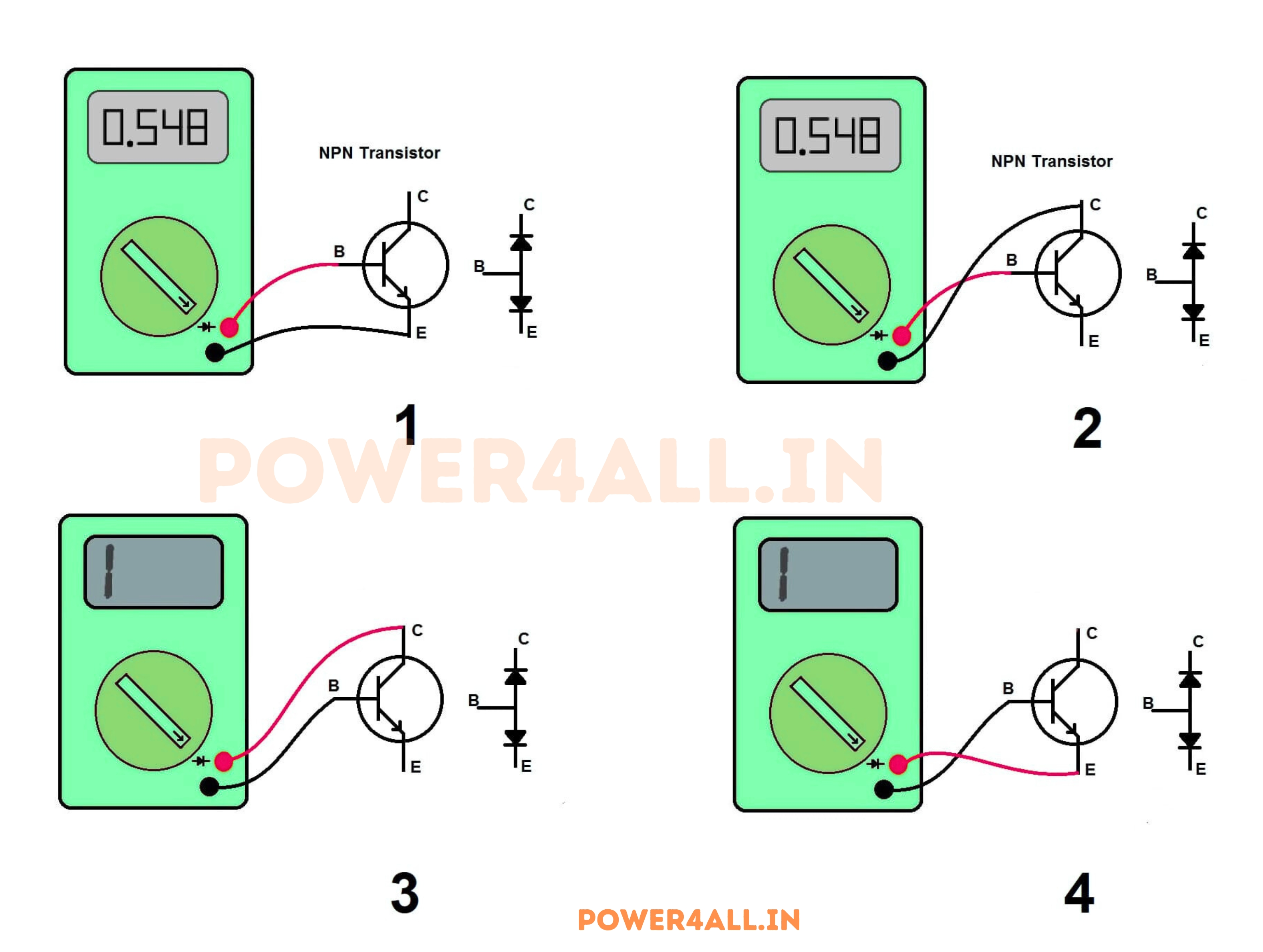
Multimeter Testing
Simple tests using a digital multimeter
Diode Test Method
NPN Test Results
- Red probe to base, black to emitter: ~0.7V
- Black probe to base, red to emitter: OL
- Red probe to base, black to collector: ~0.7V
- Black probe to base, red to collector: OL
- Between collector and emitter: OL both ways
Resistance Test Method
- Less reliable: Results vary with meter voltage
- Forward bias: Should show low resistance (few kΩ)
- Reverse bias: Should show very high resistance
- Collector-emitter: Very high resistance both ways
In-Circuit Testing
Testing transistors while still in the circuit
Voltage Measurements
- Base voltage: Should be ~0.7V above emitter for NPN
- Collector voltage: Between emitter and supply voltage
- Emitter voltage: Reference point for other measurements
- Supply voltage: Verify correct power supply operation
Normal Operating Voltages
NPN transistor in CE amplifier (12V supply):
- Collector: 6V (half supply for maximum swing)
- Base: 2.2V (bias voltage)
- Emitter: 1.5V (0.7V below base)
- VCE: 6V - 1.5V = 4.5V (active region)
Current Measurements
- Collector current: Measure voltage across emitter resistor
- Base current: Usually too small to measure directly
- Beta calculation: β = IC/IB if both can be measured
- Supply current: Total circuit current draw
Transistor Curve Tracer
Advanced testing with characteristic curve display
Curve Tracer Capabilities
- Output characteristics: IC vs VCE family of curves
- Input characteristics: IB vs VBE curves
- Beta measurement: Current gain at various operating points
- Breakdown voltages: VCEO, VCBO measurements
- Leakage currents: ICEO, ICBO at specified voltages
Information from Curves
- Linearity: How linear the active region is
- Saturation voltage: VCE(sat) from the curves
- Early voltage: Output conductance in active region
- Safe operating area: Power dissipation limits
- Thermal effects: Changes with temperature
Common Failure Modes
Typical BJT Failures and Their Symptoms
Complete Failures
| Failure Type | Symptoms | Likely Causes | Test Results |
|---|---|---|---|
| Open Base | No collector current, high collector voltage | Overvoltage, ESD damage, wire bond failure | Base appears disconnected from junctions |
| Open Collector | No collector current, base-emitter still conducts | Overcurrent, thermal stress, wire bond failure | Collector appears disconnected |
| Open Emitter | No emitter current, unusual voltage readings | Overcurrent, thermal stress, bonding failure | Emitter appears disconnected |
| Shorted B-E | Base and emitter at same potential | Overvoltage, forward bias overstress | Low resistance between base and emitter |
| Shorted C-E | Collector and emitter shorted together | Overcurrent, thermal runaway, overvoltage | Low resistance between collector and emitter |
Partial Failures
Reduced Beta
Current gain decreases due to crystal damage, contamination, or aging. Symptoms include reduced performance and changed bias point.
Increased Leakage
Higher ICEO current due to thermal damage or contamination. Causes bias point drift and thermal instability.
Noise Increase
Excessive noise due to crystal defects or contamination. More noticeable in low-level signal applications.
Frequency Degradation
Reduced fT due to junction damage. Affects high-frequency performance and switching speed.
Systematic Troubleshooting Approach
Step-by-Step Diagnosis
Essential Test Equipment
- Digital multimeter: Voltage, current, resistance, diode test
- Oscilloscope: Waveform analysis, timing, noise
- Function generator: Test signals, frequency response
- Power supply: Variable DC, current limiting
- Transistor tester: Beta, leakage, characteristic curves
Troubleshooting Examples
Problem: No Output Signal
Amplifier circuit with no AC output
Diagnostic Steps
- Check DC bias: Verify Q-point is in active region
- Test input signal: Confirm signal is reaching base
- Check coupling capacitors: May be open or wrong value
- Verify load: Output load may be too heavy
- Test transistor: May have failed or degraded
Common Causes
- Open coupling capacitor (no signal transfer)
- Wrong bias point (cutoff or saturation)
- Shorted transistor junction
- Open circuit in signal path
- Insufficient input signal level
Problem: Thermal Runaway
Transistor gets hot and draws excessive current
Symptoms
- Excessive heating: Transistor becomes very hot
- Current increase: Collector current keeps rising
- Voltage drift: Operating point shifts with temperature
- Eventual failure: Transistor may be destroyed
Solutions
- Add emitter degeneration: Emitter resistor for stability
- Improve heat sinking: Better thermal management
- Use temperature compensation: Thermistor or diode compensation
- Reduce power dissipation: Lower operating current
- Current limiting: Add current limiting circuit
Problem: Distorted Output
Output signal is clipped or non-linear
Types of Distortion
- Top clipping: Q-point too low, enters saturation
- Bottom clipping: Q-point too high, enters cutoff
- Crossover distortion: Push-pull amplifier bias problem
- Thermal distortion: Temperature-dependent bias shift
Distortion Solutions
- Adjust bias point to center of active region
- Reduce input signal level
- Increase supply voltage for more headroom
- Add negative feedback for linearity
- Use better thermal management
BJT Safety Considerations
Working with BJTs and their associated circuits requires understanding safety considerations for both the components and the people working with them. Proper safety practices protect both equipment and personnel while ensuring reliable circuit operation.
ESD Protection
Electrostatic Discharge Risks
BJTs are sensitive to static electricity damage
ESD Sensitivity Levels
- Power BJTs: 200-2000V ESD tolerance
- Small signal BJTs: 100-1000V ESD tolerance
- RF BJTs: 50-500V ESD tolerance (most sensitive)
- Human body model: Can generate 25,000V static
- Machine model: Can generate 200-4000V
ESD Damage Mechanisms
- Junction damage: Breakdown of p-n junctions
- Metal migration: Movement of metal in conductors
- Wire bond failure: Damage to internal connections
- Oxide damage: Breakdown of insulating layers
- Latent damage: Partial damage that causes later failure
ESD Protection Methods
Preventing electrostatic discharge damage
Personal Protection
- Wrist straps: Connect to earth ground, 1MΩ resistor for safety
- ESD shoes: Conductive or dissipative footwear
- Anti-static clothing: Conductive fibers prevent charge buildup
- Grounding: Touch grounded metal before handling components
Work Area Protection
- ESD mats: Dissipative work surface, properly grounded
- Ionizers: Neutralize static charges in the air
- Humidity control: 40-60% RH reduces static buildup
- Conductive containers: Store components in ESD-safe packaging
ESD Safety
Never connect wrist straps directly to ground without a 1MΩ current-limiting resistor. This protects you from electrical shock while providing ESD protection for components.
Thermal Safety
Heat-Related Hazards
Power BJTs can reach dangerous temperatures during operation, posing burn risks and potential fire hazards if not properly managed.
Temperature Dangers
- Burn hazard: Surfaces >60°C can cause burns
- Component damage: Overheating destroys transistors
- Fire risk: Overheated components can ignite
- Adjacent components: Heat affects nearby parts
- PCB damage: High temperatures damage board materials
Safe Temperature Guidelines
- Touch temperature: <40°C safe for brief contact
- Case temperature: <85°C for reliability
- Junction temperature: <125°C for silicon BJTs
- PCB temperature: <100°C to prevent delamination
- Component spacing: Allow airflow around hot parts
Electrical Safety
High Voltage Precautions
Safety when working with high-voltage BJT circuits
Voltage Hazards
- Shock hazard: >50V can be dangerous
- Arc flash: High current can cause arc flash
- Stored energy: Capacitors remain charged
- Inductive kickback: Motors and transformers generate spikes
- Ground faults: Improper grounding creates hazards
High Voltage Safety Rules
- Always de-energize circuits before working
- Use lockout/tagout procedures
- Verify zero energy with meter
- Discharge capacitors safely before handling
- Use appropriate PPE for voltage levels
- Never work alone on high-voltage systems
- Keep emergency contacts readily available
Fire and Burn Prevention
Preventing fires and thermal injuries from overheated components
Fire Prevention
- Proper fusing: Use appropriate fuses and circuit breakers
- Current limiting: Ensure circuits cannot draw excessive current
- Ventilation: Provide adequate airflow around hot components
- Component spacing: Keep flammable materials away from heat sources
- Emergency shutdown: Have quick disconnect capability
Burn Prevention
- Warning labels: Mark hot surfaces and high-power components
- Cooling time: Allow components to cool before handling
- Insulated tools: Use insulated handles when necessary
- Protective barriers: Cover hot surfaces to prevent accidental contact
Frequently Asked Questions About BJTs
Common questions about BJT transistors, their operation, applications, and troubleshooting. These answers address the most frequent concerns from students, hobbyists, and engineers working with BJT technology.
Basic Operation and Theory
Q: What's the main difference between NPN and PNP transistors?
A: The main differences are in current direction and biasing. In NPN transistors, conventional current flows from collector to emitter when the base is positive relative to the emitter. In PNP transistors, current flows from emitter to collector when the base is negative relative to the emitter. Think of NPN as "Not Pointing iN" (arrow points out) and PNP as "Pointing iN" (arrow points in).
Q: Why is the base region so thin in a BJT?
A: The base must be very thin (typically 1-10 micrometers) to ensure that most charge carriers from the emitter pass through to the collector without recombining in the base. If the base were thick, too many carriers would recombine, reducing the current gain (β) and making the transistor inefficient. The thin base is what enables the current amplification effect.
Q: What does "bipolar" mean in Bipolar Junction Transistor?
A: "Bipolar" means that the device uses both types of charge carriers: electrons (negative) and holes (positive). This is in contrast to unipolar devices like FETs, which primarily use only one type of charge carrier. In a BJT, both electrons and holes contribute to the current flow, depending on whether it's NPN or PNP.
Q: Can I substitute an NPN transistor with a PNP transistor?
A: Not directly, because they require opposite bias polarities. However, you can often redesign the circuit to use the opposite type by reversing supply polarities and adjusting the biasing network. The electrical parameters (β, voltage ratings, current capacity) should be similar for proper substitution.
Practical Applications and Design
Q: How do I calculate the base resistor for a switching application?
A: For reliable switching, ensure the transistor is driven into saturation. Calculate the base current needed for saturation: IB(sat) = IC(desired) / β(min). Then add a safety factor of 2-3 times. Base resistor = (VCC - VBE) / (IB(sat) × safety factor). For example, switching 100mA with β=100: IB(sat) = 1mA, with 3× safety factor = 3mA, so RB = (5V - 0.7V) / 3mA = 1.43kΩ, use 1.2kΩ or 1kΩ.
Q: Why do my BJT amplifiers have distortion?
A: Common causes include: (1) Improper bias point - should be in the center of the active region for maximum signal swing, (2) Input signal too large - causing clipping at supply rails, (3) Insufficient power supply voltage - not enough headroom for signal swing, (4) Temperature drift - changing the operating point, (5) Nonlinear operation - operating near cutoff or saturation regions. Check your bias voltages and reduce input signal amplitude if necessary.
Q: What's the difference between BJTs and MOSFETs for switching?
A: BJTs are current-controlled (base current controls collector current) while MOSFETs are voltage-controlled (gate voltage controls drain current). MOSFETs have higher input impedance, faster switching speeds, and no continuous gate current. BJTs typically have lower on-resistance and better linearity. For low-frequency, high-current applications, BJTs may be preferred. For high-frequency or low-power applications, MOSFETs are often better.
Q: How do I prevent thermal runaway in power BJTs?
A: Use these techniques: (1) Emitter degeneration - add a small resistor in series with the emitter, (2) Adequate heat sinking - keep junction temperature low, (3) Current limiting - use current limiting circuits, (4) Temperature compensation - use thermistors or diodes to compensate for temperature effects, (5) Negative feedback - helps stabilize the operating point. For high-power applications, consider using multiple BJTs in parallel with individual emitter resistors.
Troubleshooting and Repair
Q: How can I tell if a BJT is faulty?
A: Use a multimeter's diode test mode: (1) Test base-emitter junction - should show ~0.6-0.7V forward, open circuit reverse, (2) Test base-collector junction - should show ~0.6-0.7V forward, open circuit reverse, (3) Test collector-emitter - should show open circuit in both directions when base is not connected. Any short circuits or open circuits in the junctions indicate a failed transistor. You can also measure β using a transistor tester if available.
Q: My amplifier circuit has no output. Where do I start troubleshooting?
A: Follow this systematic approach: (1) Check power supply voltages, (2) Measure DC bias voltages on the transistor (VB, VC, VE), (3) Verify the transistor is in the active region (VCE > VBE), (4) Check input signal is reaching the base, (5) Test the transistor with a multimeter, (6) Verify all component values and connections, (7) Check for short circuits or open circuits in the signal path. Most problems are due to incorrect biasing or faulty components.
Q: Why does my BJT get very hot during operation?
A: Excessive heating usually indicates: (1) Too much current - check if the transistor is being overdriven, (2) High power dissipation - verify that VCE × IC is within the power rating, (3) Poor heat sinking - ensure adequate thermal management, (4) Wrong operating region - transistor may be in linear region when it should be switching, (5) Oscillation - high-frequency oscillation can cause heating, (6) Thermal runaway - positive feedback causing runaway heating. Measure currents and voltages to identify the cause.
Q: Can temperature affect BJT performance significantly?
A: Yes, temperature has major effects: (1) VBE decreases by ~2mV/°C, shifting the bias point, (2) β typically increases with temperature, changing gain, (3) Leakage currents double approximately every 10°C, (4) Thermal runaway becomes possible in power applications. For critical applications, use temperature compensation (thermistors, matched diodes) or choose circuits with inherent temperature stability like voltage divider biasing with emitter degeneration.
Selection and Design Guidelines
Q: How do I choose between different BJT types for my application?
A: Consider these factors: (1) Frequency: For audio (20Hz-20kHz), general purpose BJTs work; for RF (MHz+), choose high fT devices, (2) Power: Small signal (<1W) vs power BJTs (>1W), (3) Precision: Low noise, matched pairs for precision applications, (4) Cost: General purpose for non-critical applications, (5) Package: Through-hole for prototyping, SMD for production. Start with common types like 2N2222 (NPN) or 2N2907 (PNP) for general applications.
Q: What's the difference between small signal and power BJTs?
A: Small signal BJTs (typically <1W) are optimized for voltage and current amplification with parameters like high β, low noise, and good frequency response. Power BJTs (>1W) are designed for high current handling with features like larger die size, better thermal management, lower saturation voltage, and robust construction. Power BJTs often have lower β but can handle much higher currents and power dissipation.
Q: When should I use a Darlington pair instead of a single BJT?
A: Use Darlington pairs when you need: (1) Very high current gain (β can be >1000), (2) High input impedance, (3) Low input current requirements. Drawbacks include: slower switching speed, higher saturation voltage (~1.4V), and reduced bandwidth. Darlington pairs are excellent for interfacing logic circuits to high-current loads like motors and relays, but avoid them in high-frequency or precision switching applications.
Q: How important is the β (current gain) specification?
A: β importance depends on the application: (1) Critical in linear amplifiers: Affects gain and input impedance, (2) Less critical in switching: As long as you can drive the transistor into saturation, (3) Variable parameter: β varies with temperature, current, and between devices, (4) Design for worst case: Use minimum β values for calculations. Good circuit design should work reliably even with wide β variations (2:1 or 3:1 range).
Conclusion: Mastering BJT Transistor Technology
BJT transistors remain fundamental building blocks of modern electronics, despite the rise of newer technologies like MOSFETs. Understanding BJTs provides essential insights into semiconductor physics, amplification principles, and switching concepts that apply to all areas of electronics design.
Key Takeaways
Fundamental Understanding
BJTs demonstrate the core principles of semiconductor operation, current control, and amplification that form the foundation of all electronics.
Practical Applications
From simple switches to complex amplifiers, BJTs provide reliable, cost-effective solutions for countless electronic applications.
Design Principles
Proper biasing, thermal management, and circuit design principles learned with BJTs apply to all active semiconductor devices.
Safety Awareness
Understanding electrical safety, ESD protection, and thermal management ensures safe and reliable circuit operation.
BJTs in Modern Electronics
Current Applications
Where BJTs excel in today's technology
- Analog circuits: Audio amplifiers, operational amplifiers, precision references
- Power control: Motor drivers, power supplies, linear regulators
- RF applications: High-frequency amplifiers, oscillators, mixers
- Interface circuits: Logic level conversion, sensor conditioning
- Discrete solutions: Where integrated circuits are impractical
Advantages Over Newer Technologies
Why BJTs remain relevant
- Cost effectiveness: Simple, mature manufacturing processes
- High current capability: Excellent for power applications
- Linear operation: Superior for precision analog circuits
- Temperature characteristics: Predictable behavior over wide ranges
- ESD robustness: More resistant to static damage than MOSFETs
Future Developments
Evolution of BJT technology
- SiGe technology: Higher frequency operation, improved performance
- Advanced packaging: Better thermal management, smaller sizes
- Specialized designs: Optimized for specific applications
- Integration: BJTs combined with other technologies on single chips
- New materials: Gallium arsenide and other compound semiconductors
Learning Path and Next Steps
Building on BJT Knowledge
Understanding BJTs provides an excellent foundation for learning other semiconductor devices and advanced electronic concepts.
Practical Recommendations
- Hands-on practice: Build circuits to reinforce theoretical knowledge
- Simulation tools: Use SPICE simulators to explore BJT behavior
- Component experimentation: Try different BJT types in the same circuit
- Measurement skills: Learn to use oscilloscopes and other test equipment
- Design challenges: Set goals like building specific amplifiers or switches
- Community involvement: Join electronics forums and maker communities
Final Thoughts
BJT transistors represent one of humanity's greatest technological achievements. From their invention in 1947 to their continued use in modern electronics, they have enabled the digital revolution, space exploration, telecommunications, and countless other advances that define our modern world.
Whether you're a student learning electronics fundamentals, a hobbyist building projects, or an engineer designing professional systems, understanding BJTs gives you powerful tools for creating and controlling electronic circuits. The principles you learn - current control, amplification, switching, and thermal management - apply throughout electronics and will serve you well as technology continues to evolve.
Remember
The best way to truly understand BJTs is through hands-on experimentation. Start with simple circuits, measure voltages and currents, observe how changes affect operation, and gradually work up to more complex applications. Each circuit you build deepens your understanding and builds your confidence in working with these remarkable devices.
Thank you for taking this comprehensive journey through BJT transistor technology!
Armed with this knowledge, you're ready to design, analyze, and troubleshoot BJT circuits with confidence and skill.