Single Phase Half-Bridge Inverter
A single-phase half-bridge inverter is designed to transform DC input into a two-level AC output, commonly used in low and medium power applications.
Single Phase Inverter
A single-phase inverter is a device designed to transform a DC voltage source into a single-phase AC output voltage at a specified frequency and voltage level. It employs a switching process to accomplish the conversion from DC input to AC output a nd is categorized as a phase-commutated inverter when operating in the inverter mode. Specifically, when operating in the inverter mode, phase-commutated inverters are commonly referred to as line-commutated inverters. It is worth noting that line-commutated inverters necessitate an existing AC supply at their output terminals for the commutation process.
Types of Single-Phase Inverter
- Half-Bridge Inverter: Utilizes two switches and produces a two-level AC output. It is simple and cost-effective, making it suitable for low to medium power applications.
- Full-Bridge Inverter: Employs four switches to create a more efficient and flexible AC output. This topology is commonly used in higher power applications.
Single Phase Half-Bridge Inverter
The half-bridge inverter architecture is a foundational component of single-phase inverters, adept at converting direct current into alternating current with efficiency and precision. This structure comprises two switch elements, typically transistors, IGBTs, or MOSFETs, arranged in series across a DC voltage source. Additionally, two feedback diodes and two capacitors establish connections between the source and load. Within this arrangement, the load is strategically positioned between the midpoint of the capacitors and the midpoint of the diodes and switches. Through complementary switching operations of the components, an alternating current output voltage is induced across the load. Notably, feedback diodes play a crucial role, especially with inductive loads, ensuring a controlled and seamless current flow.
The half-bridge inverter is particularly advantageous for applications requiring moderate power levels, such as in small-scale renewable energy systems, motor drives, and uninterruptible power supplies (UPS). Its design allows for efficient operation, reduced component count, and cost-effectiveness, making it a popular choice in various industrial and commercial applications.
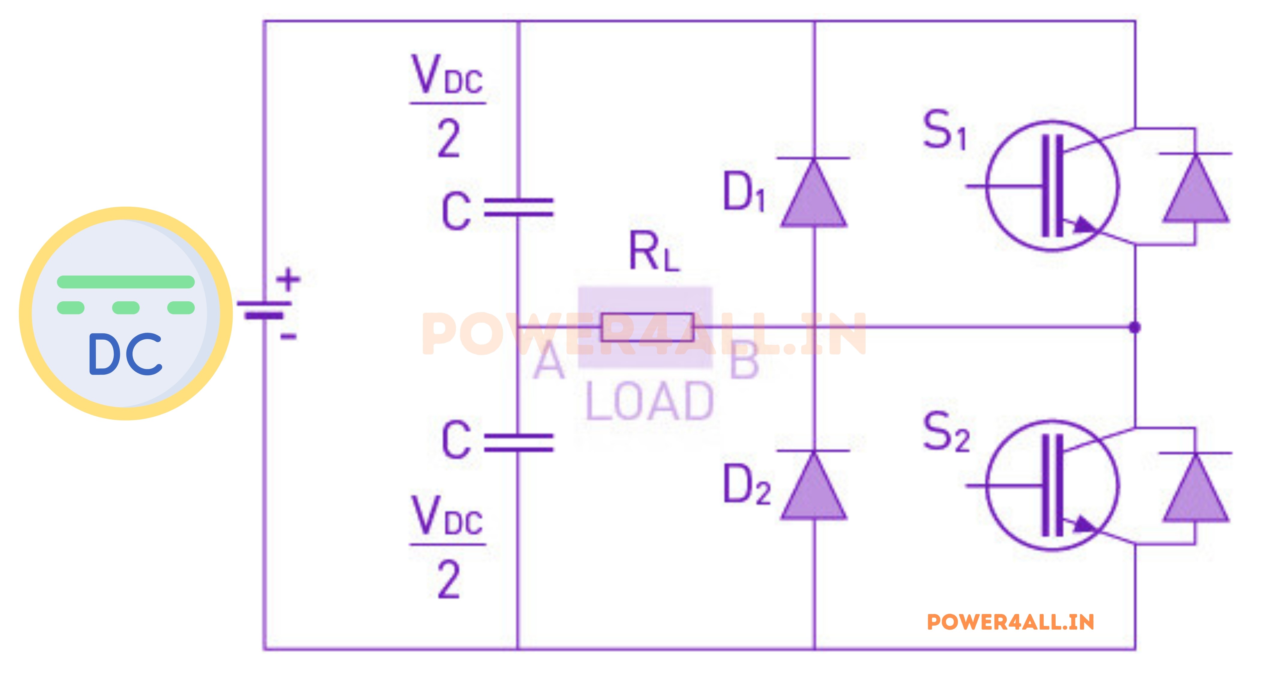
Half Bridge Inverter with Resistive Load
The half-bridge inverter architecture, illustrated in the figure below, represents a foundational single-phase inverter structure. It comprises two switching components (typically transistors, IGBTs, or MOSFETs) connected in series across a DC voltage source, along with two feedback diodes and two capacitors that establish the connection between the source and load.
The load is positioned between the midpoint of the capacitors (A node) and the midpoint of the diodes and switches (B node). This arrangement results in the generation of an AC output voltage across the load through the complementary operation of the switches.
Notably, feedback diodes are integrated when inductive loads are employed. While the half-bridge inverter presents a relatively simple and cost-effective solution, it necessitates a center-tapped DC voltage source or a split capacitor to fulfill the voltage requirements.
Working of Single-Phase Half Bridge Inverter with Resistive Load
The two modes of operation for a half-bridge inverter with R load are as discussed below
Mode-1: Switch S1 ON and S2 OFF
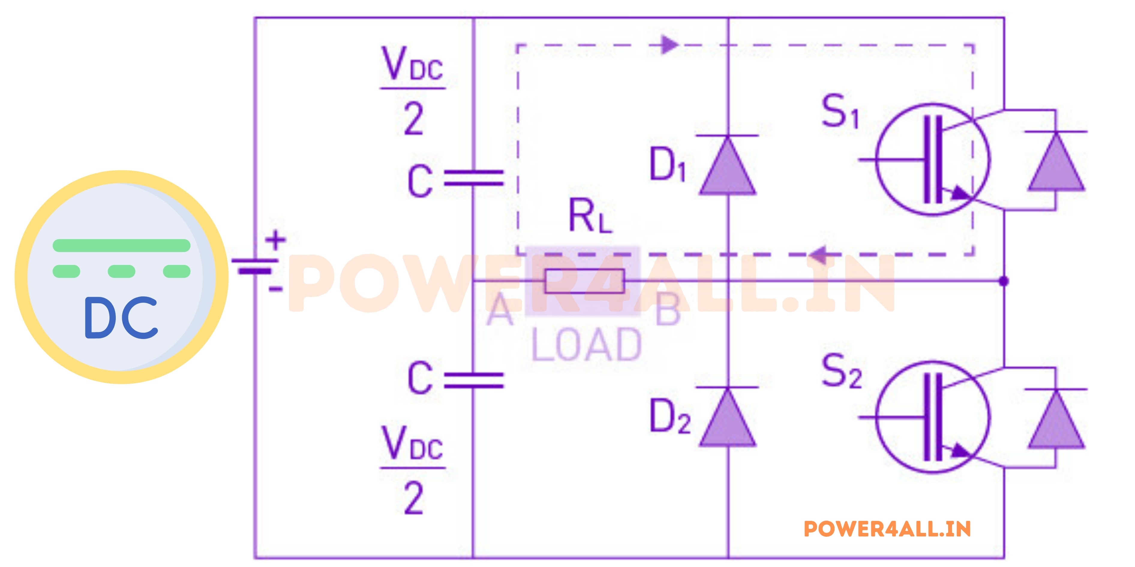
The diagram above illustrates Mode-1 operation of a half H-bridge inverter with a resistive load. In this configuration, the output voltage is precisely half of the DC source voltage. Current is directed through the load and the upper switch (S1), while the lower switch (S2) remains in an off state. The measurement of the output voltage across the load can be conducted as:
Vout = Vdc/2
Mode-2: Switch S1 OFF and S2 ON
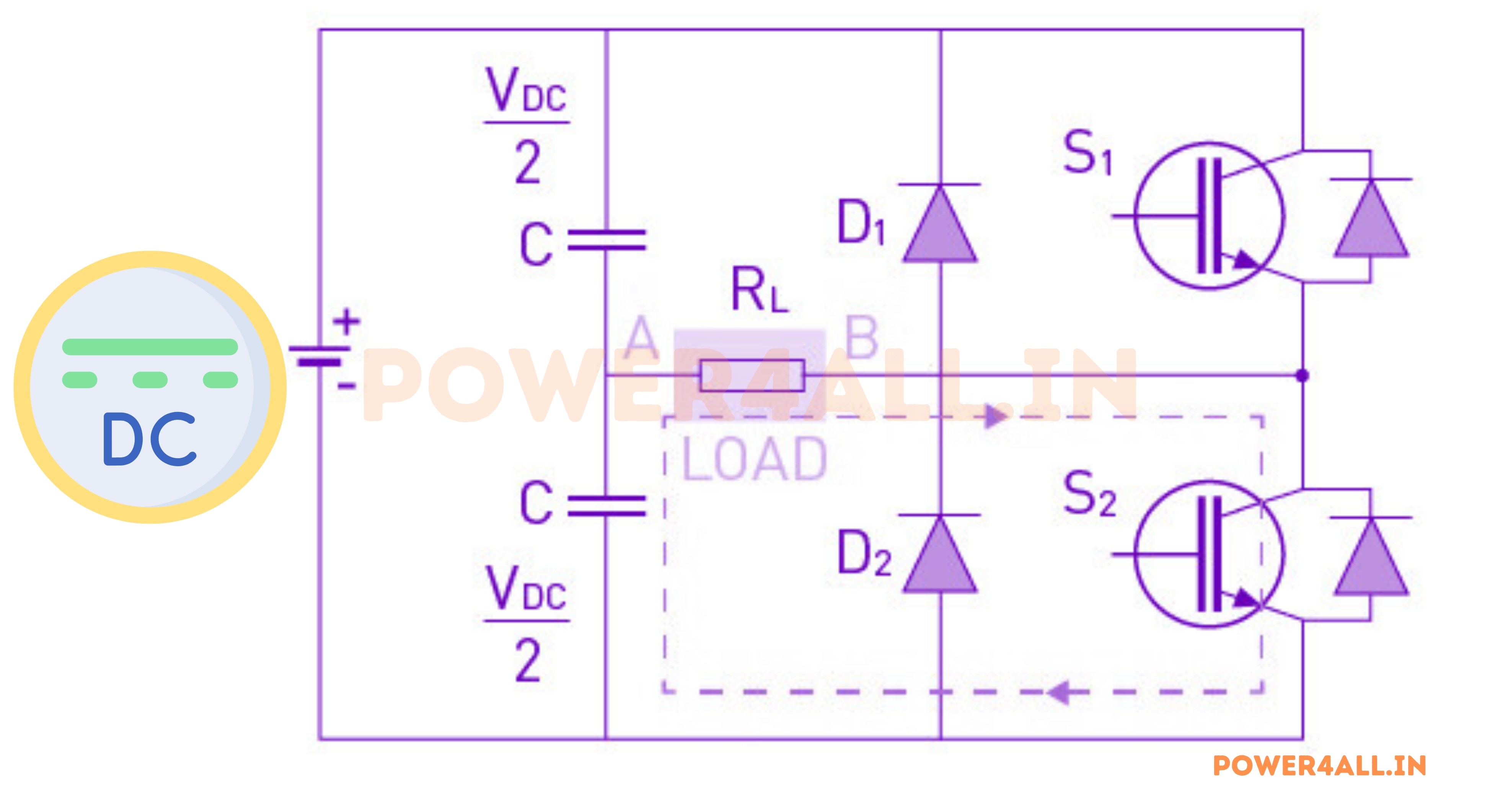
The diagram above illustrates Mode-2 operation of a half H-bridge inverter with a resistive load. In this configuration, the output voltage is precisely half of the DC source voltage. Current is directed through the load and the lower switch (S2), while the upper switch (S1) remains in an off state. The measurement of the output voltage across the load can be conducted as:
Vout = -Vdc/2
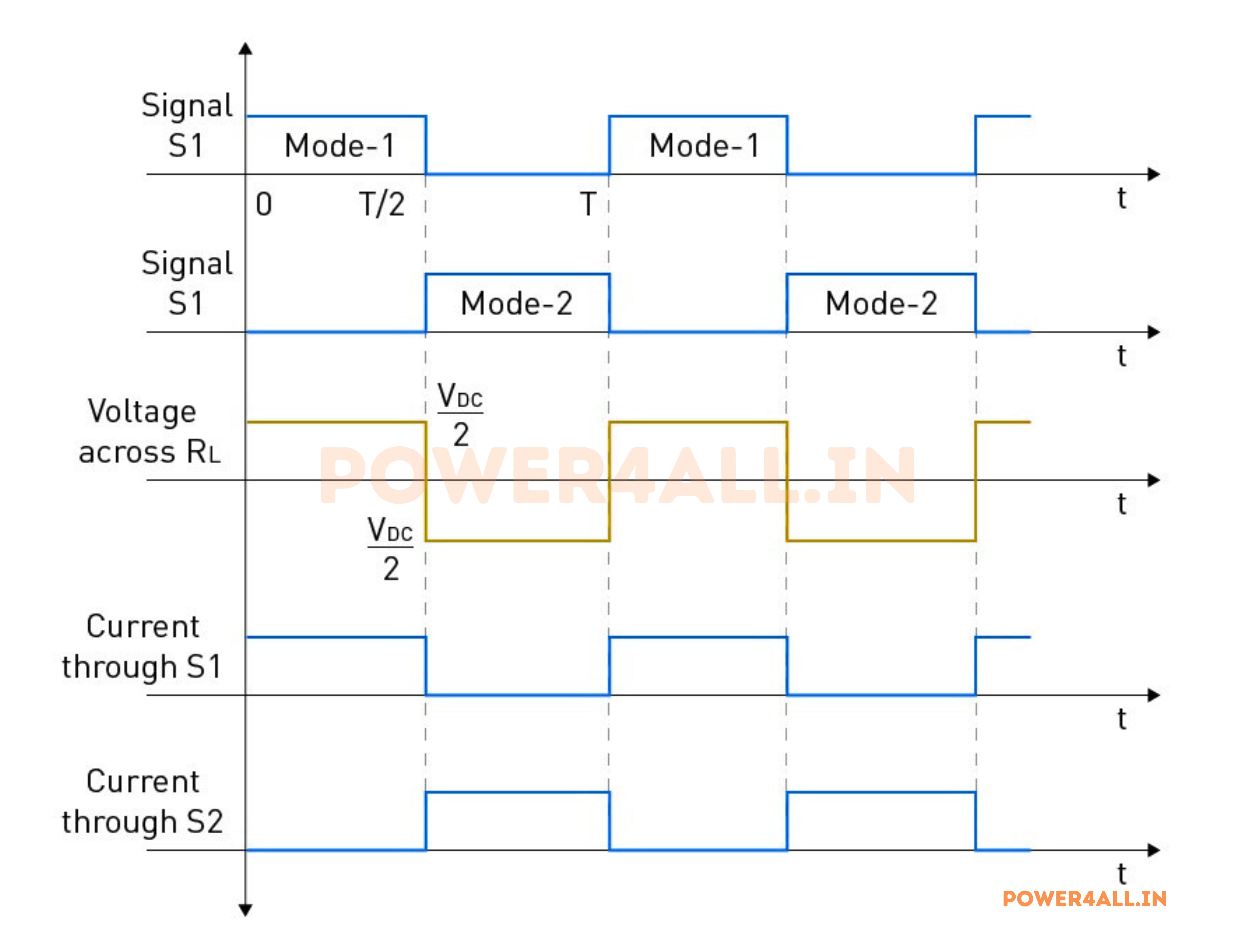
The output voltage waveform of the half-bridge inverter is illustrated in the figure below. The output voltage alternates between +Vdc/2 and -Vdc/2, resulting in a square wave output voltage.
Waveform of Half Bridge Inverter with R Load
The output voltage waveform of the half-bridge inverter is illustrated in the figure below. The output voltage alternates between +Vdc/2 and -Vdc/2, resulting in a square wave output voltage.
Advantages
- Simple Circuit Design: The half-bridge inverter uses a basic circuit with fewer components, making it easy to design and understand.
- Cost-Effective: Fewer components mean lower manufacturing and maintenance costs, making it suitable for budget-sensitive applications.
- Compact and Lightweight: The simple structure allows for a smaller, lighter inverter that can be easily installed in space-constrained areas.
- Good for Low Power Applications: It is ideal for applications that do not require high power, such as small UPS systems, basic motor drives, and educational experiments.
- Efficient for Resistive Loads: Performs well with purely resistive loads, providing a clear square wave output.
- Foundation for Learning: Often used in teaching and laboratory settings to introduce inverter concepts.
Disadvantages
- Limited Power Handling: Not suitable for high-power applications; power output is lower compared to full-bridge inverters.
- Requires 3-Wire DC Supply: Needs a split DC supply or two capacitors for proper operation, adding complexity to the power source.
- High Harmonic Distortion: The output is a square wave, which contains significant harmonics and can cause issues with sensitive or inductive loads.
- Capacitor Balancing Needed: Requires careful balancing of capacitors to maintain stable operation and avoid voltage drift.
- Not Ideal for Inductive Loads: Without freewheeling diodes, performance with inductive loads is poor; additional components are needed for such cases.
- Lower Efficiency with Reactive Loads: More losses and less efficient when driving loads that are not purely resistive.
- Limited Output Waveform Quality: The square wave output may not be suitable for all applications, especially those requiring a pure sine wave.
- Noise and EMI Issues: The switching action can generate electrical noise and electromagnetic interference, which may affect nearby electronics.