Complete MOSFET Mastery Guide
Master Metal Oxide Semiconductor Field Effect Transistors - from basic principles and construction to advanced switching applications in modern electronics and power systems
Complete Learning Path - MOSFET Fundamentals to Applications
Navigate through comprehensive coverage of MOSFETs from basic principles to advanced power electronics applications
What is a MOSFET (Metal Oxide Semiconductor Field Effect Transistor)?
A MOSFET (Metal Oxide Semiconductor Field Effect Transistor) is a voltage-controlled semiconductor device that forms the foundation of modern electronics. It's a three-terminal device (gate, source, drain) that can switch or amplify electrical signals with exceptional efficiency, making it the most widely used transistor in digital circuits, power electronics, and integrated circuits.
The Electronic Valve
Think of a MOSFET as an electronic valve controlled by an electric field. Unlike a mechanical valve that requires physical force, a MOSFET uses voltage at the gate to create an electric field that controls current flow between source and drain - with virtually no current flowing into the gate itself.
Water Valve Analogy
- Gate voltage → Valve handle position
- Source-drain current → Water flow through pipe
- Electric field control → Smooth valve operation
- No gate current → No energy needed to hold valve position
Metal + Oxide + Semiconductor = MOSFET
Three-layer structure enables voltage-controlled operation
Why MOSFETs Revolutionized Electronics
MOSFETs transformed electronics by offering unprecedented efficiency, speed, and scalability. Before MOSFETs, electronic switching relied on bipolar transistors and vacuum tubes, which consumed more power and were larger. MOSFETs enabled the digital revolution by allowing billions of transistors on a single chip.
Ultra-High Input Impedance
Gate input impedance exceeds 10¹⁴ Ω, meaning virtually no current flows into the gate, enabling very low power operation and easy interfacing.
Fast Switching Speed
MOSFETs can switch in nanoseconds or even picoseconds, enabling high-frequency operation and rapid digital switching in modern processors.
Voltage Control
Unlike current-controlled BJTs, MOSFETs are voltage-controlled, making them easier to drive and more efficient in switching applications.
Scalability
MOSFET technology scales down to nanometer dimensions, enabling billions of transistors in modern microprocessors and memory chips.
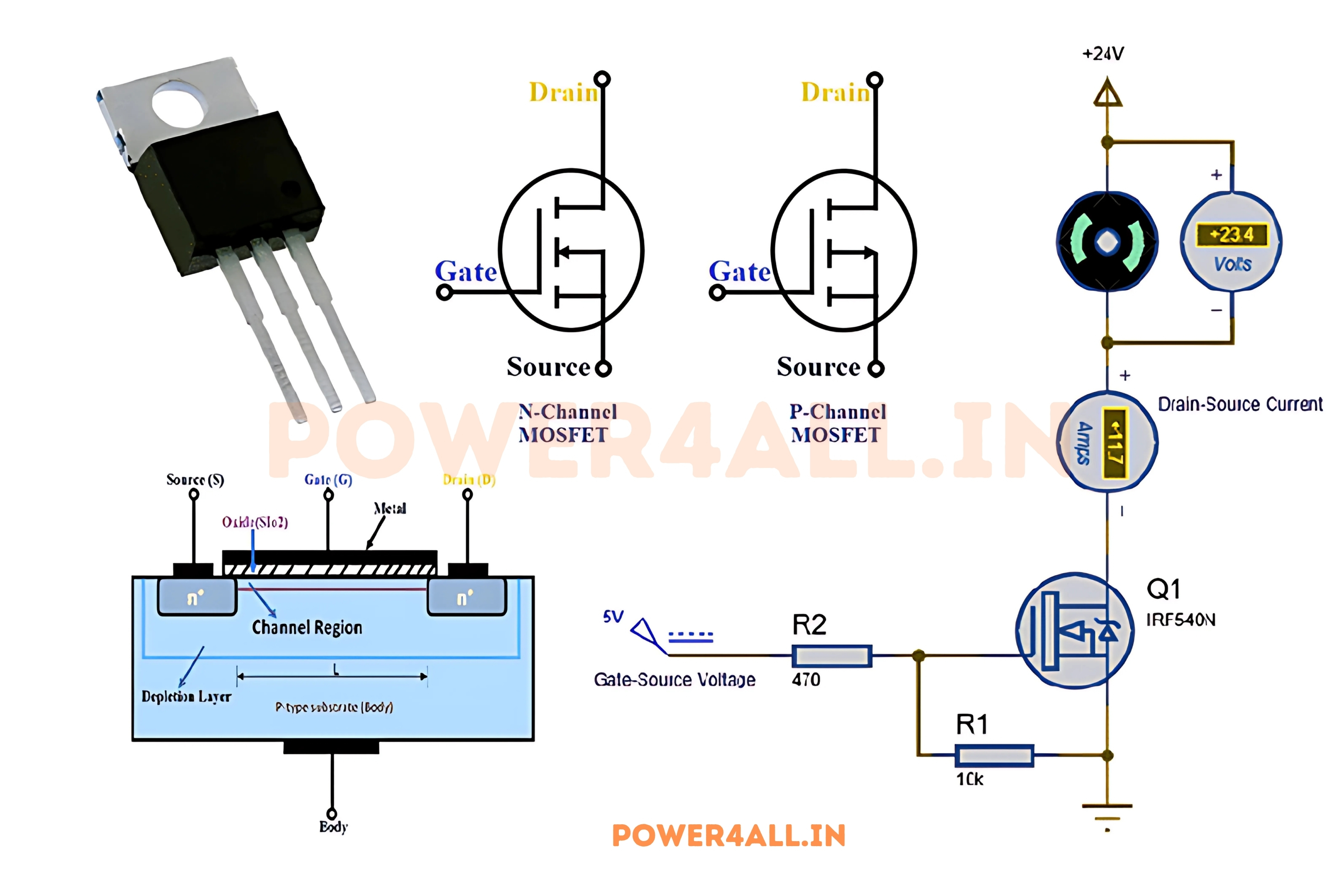
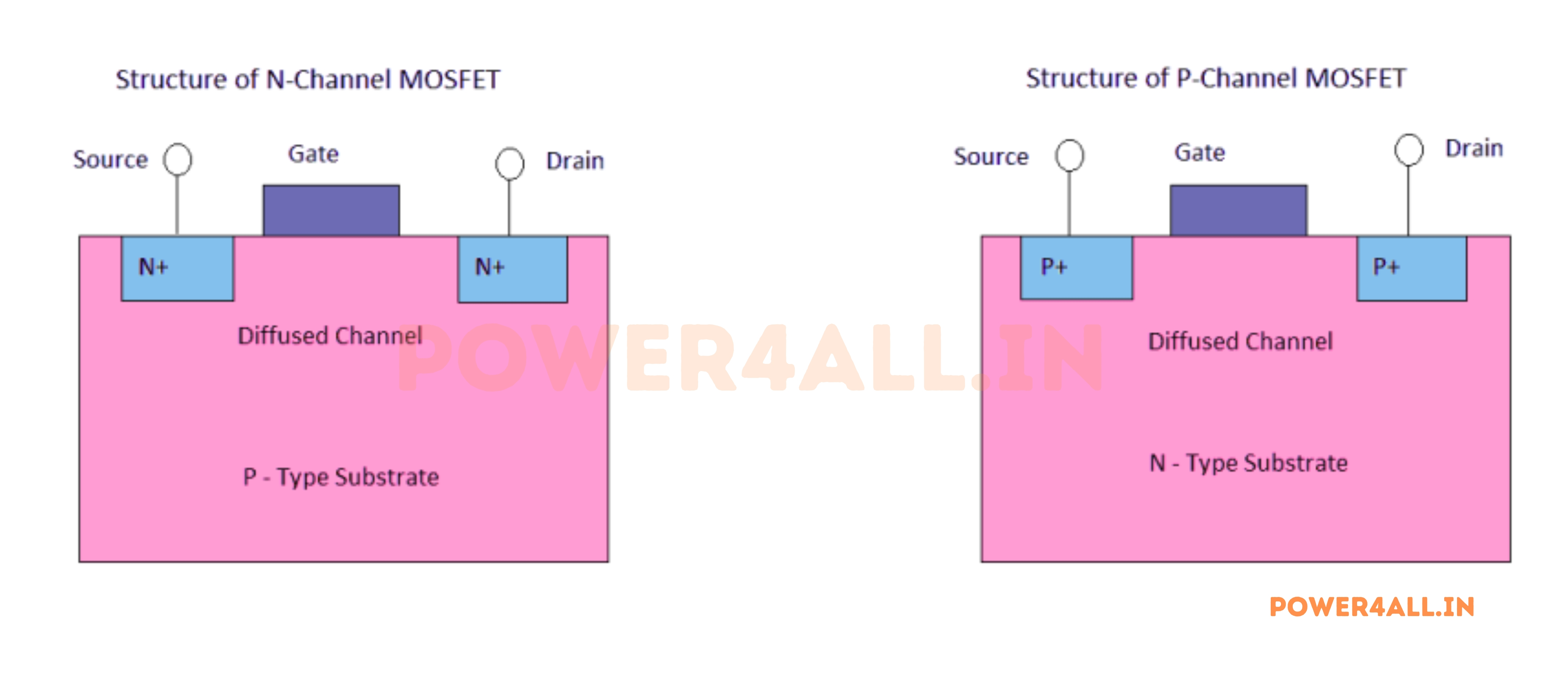
MOSFET Terminals and Symbol
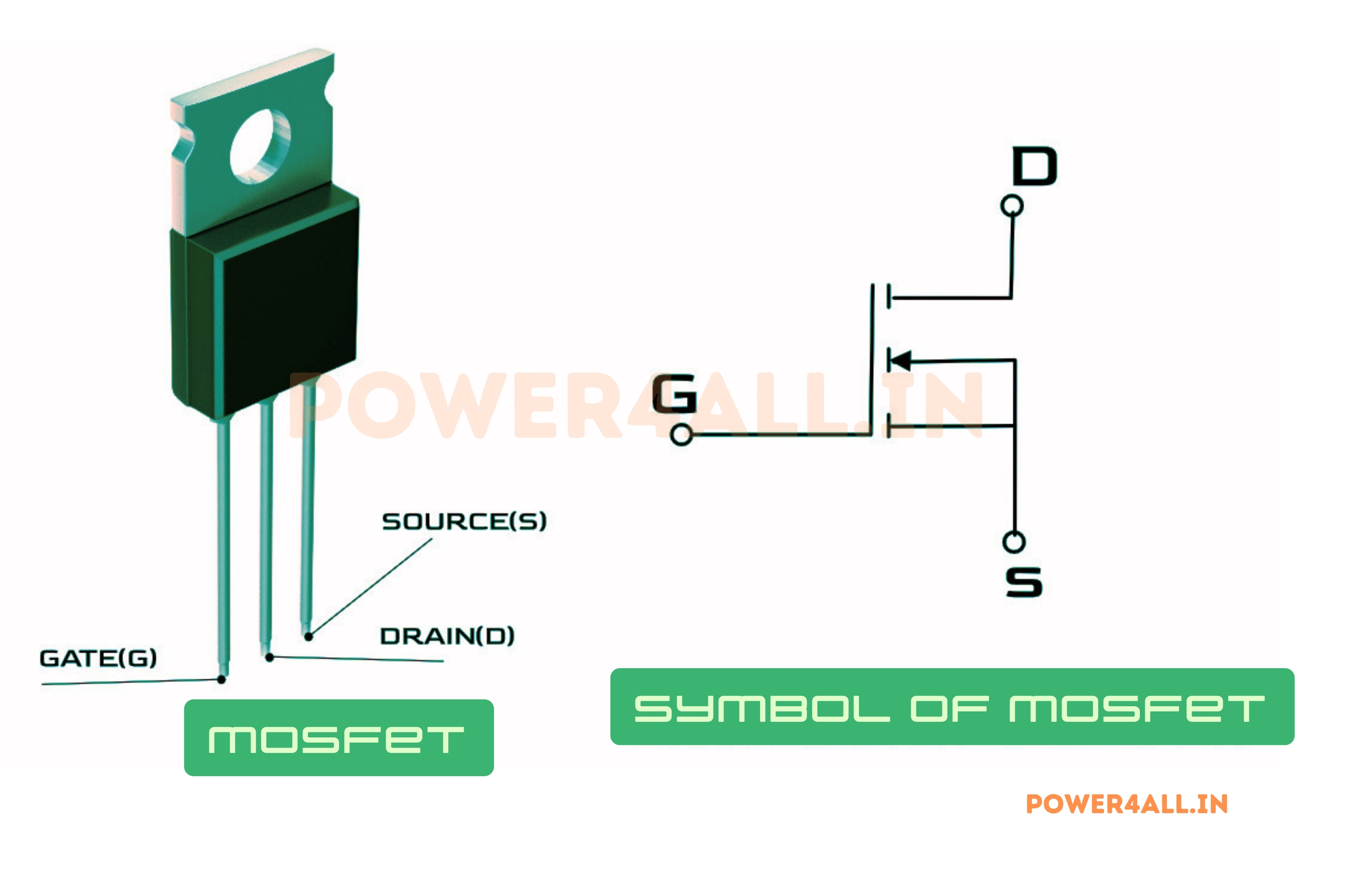
Four Terminals
- Gate (G): Control terminal, insulated from channel by oxide layer
- Source (S): Where current enters the device (like emitter in BJT)
- Drain (D): Where current exits the device (like collector in BJT)
- Body/Substrate (B): Usually connected to source in discrete devices
- Channel: Conductive path between source and drain (controlled by gate)
Operating Principle
- OFF state: No channel exists, no current flows (enhancement mode)
- Threshold voltage: Minimum gate voltage to create channel
- ON state: Channel forms, current flows proportional to gate voltage
- Saturation: Channel pinches off, current becomes constant
- Bidirectional: Can conduct in both directions when ON
MOSFETs in Everyday Electronics
- Microprocessors: Billions of MOSFETs in CPUs and GPUs
- Memory devices: Flash drives, SSDs, RAM modules
- Power supplies: Switching regulators and converters
- Motor drives: Electric vehicle controllers and robotics
- LED lighting: Dimming controls and driver circuits
- Audio amplifiers: Class-D amplifiers and switching circuits
Historical Impact
The MOSFET was invented in 1959 by Mohamed Atalla and Dawon Kahng at Bell Labs. This invention enabled the development of modern computing, smartphones, and the entire digital age. Today, over 13 trillion MOSFETs are manufactured annually, making them the most produced human artifact in history!
MOSFET Fundamentals & Physics of Operation
Understanding MOSFET operation requires exploring the Metal-Oxide-Semiconductor structure, channel formation physics, and the field effect mechanism that enables voltage-controlled operation. This physics foundation explains why MOSFETs are so effective for both analog and digital applications.
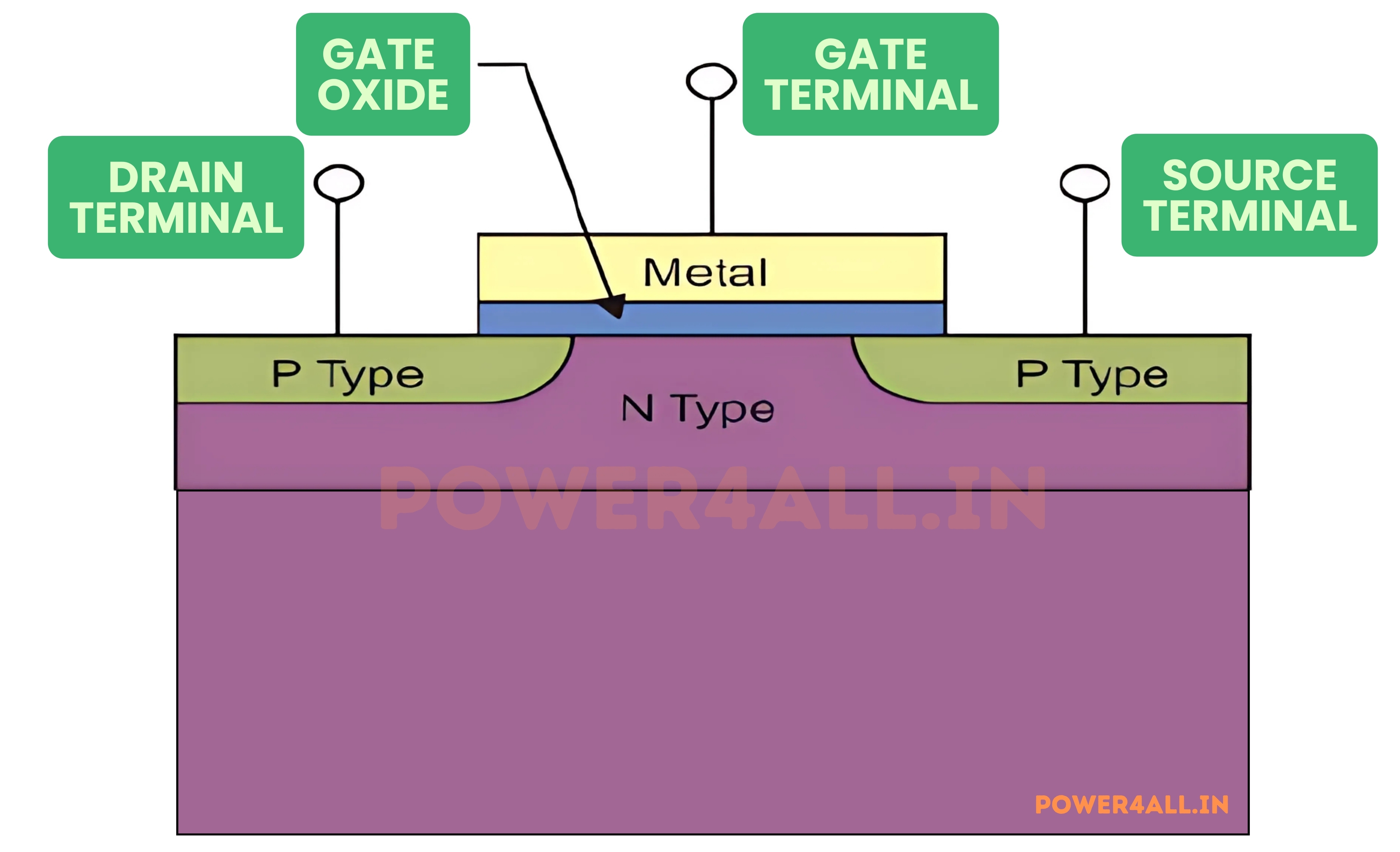
MOS Structure and Physics
Understanding the Metal-Oxide-Semiconductor Structure
Three-Layer MOS Structure
The MOSFET's operation is based on the MOS (Metal-Oxide-Semiconductor) capacitor structure, which creates an electric field to control charge carriers in the semiconductor.
| Layer | Material | Function | Typical Thickness |
|---|---|---|---|
| Metal Gate | Polysilicon | Control electrode | 200-500nm |
| Oxide Insulator | Silicon Dioxide (SiO₂) | Electric field isolation | 1-10nm (modern devices) |
| Semiconductor | Silicon substrate | Channel formation region | 10-100μm |
Electric Field Effect
MOS Capacitor
Gate and substrate form a parallel plate capacitor with oxide as dielectric. Gate voltage creates electric field across oxide.
Charge Control
Electric field attracts or repels charge carriers in semiconductor, forming or depleting the conductive channel.
Inversion Layer
Strong electric field inverts the semiconductor surface, creating a thin conductive channel for current flow.
Channel Formation Mechanism
N-Channel Enhancement MOSFET
In an N-channel device, positive gate voltage attracts electrons to the surface, forming a conductive channel between N+ source and drain regions in the P-type substrate.
Channel Formation Process
ID = μnCox(W/L)(VGS - VTH)VDS
Linear region drain current equation
Key Physics Parameters
- μn: Electron mobility in channel
- Cox: Gate oxide capacitance per unit area
- W/L: Channel width to length ratio
- VTH: Threshold voltage
- VGS: Gate-to-source voltage
- VDS: Drain-to-source voltage
MOSFET Capacitances and Switching
Understanding MOSFET Capacitances and Dynamic Behavior
Parasitic Capacitances
MOSFETs have several parasitic capacitances that affect switching speed and dynamic performance. Understanding these is crucial for high-frequency and fast switching applications.
Input Capacitances
- CGS (Gate-Source): Largest capacitance, affects turn-on speed
- CGD (Gate-Drain): Miller capacitance, causes switching delays
- CGB (Gate-Body): Usually small in enhancement MOSFETs
- CISS = CGS + CGD: Total input capacitance
Output Capacitances
- CDS (Drain-Source): Small, affects high-frequency performance
- CDB (Drain-Body): Junction capacitance, voltage dependent
- CSB (Source-Body): Usually zero (body tied to source)
- COSS = CDS + CDB: Total output capacitance
Switching Transitions
| Switching Phase | Dominant Capacitance | Time Period | Characteristics |
|---|---|---|---|
| Turn-on delay | CGS | td(on) | Gate voltage rises to threshold |
| Current rise | CGS | tr | Drain current increases |
| Voltage fall | CGD (Miller) | tf | Drain voltage decreases |
| Turn-off delay | CGS + CGD | td(off) | Gate discharges to threshold |
tsw = RG × (CGS + CGD)
Simplified switching time estimation
Temperature Effects and Reliability
Temperature Dependencies
Critical parameters that change with temperature
Key Temperature Effects
- Threshold voltage: Decreases ~2mV/°C (negative tempco)
- Carrier mobility: Decreases with temperature (T^-1.5)
- Leakage current: Doubles every 10°C increase
- ON resistance: Increases with temperature
Thermal Runaway Prevention
- MOSFETs have positive temperature coefficient of resistance
- Higher temperature → Higher RDS(on) → Less current
- Self-limiting behavior prevents thermal runaway
- Parallel MOSFETs naturally current share
Reliability Mechanisms
Understanding MOSFET degradation and lifetime
Failure Mechanisms
- Gate oxide breakdown: High electric field damage
- Hot carrier injection: High-energy carriers degrade oxide
- Negative bias temperature instability: PMOS degradation
- Electromigration: Metal migration in interconnects
Reliability Guidelines
- Gate voltage: Stay within ±20V typical maximum
- ESD protection: Critical due to thin gate oxide
- Temperature cycling: Limit thermal stress
- Safe operating area: Avoid simultaneous high V and I
ESD Sensitivity
Modern MOSFETs have extremely thin gate oxides (1-10nm) making them extremely sensitive to electrostatic discharge. Always use proper ESD protection when handling MOSFETs, and include ESD protection diodes in circuit designs.
MOSFET Construction & Physical Structure
MOSFET construction varies significantly from small-signal devices to high-power MOSFETs. Understanding the physical structure, manufacturing process, and package types is essential for proper device selection and optimal circuit design.
Silicon Fabrication Process
Manufacturing Steps
MOSFET fabrication is a precision process involving multiple photolithographic steps to create the source, drain, gate, and isolation structures with nanometer accuracy.
Modern Process Specifications
- Gate length: 5nm - 180nm (technology node)
- Gate oxide thickness: 1-5nm (few atomic layers)
- Doping concentration: 10¹⁶-10²⁰ atoms/cm³
- Channel width: 0.1μm - 10mm (design dependent)
- Junction depth: 10-200nm
Cox = εox / tox
Gate oxide capacitance per unit area
MOSFET Types by Construction
Planar MOSFETs
Traditional flat gate structure
Characteristics
- Gate structure: Flat gate over planar channel
- Scaling limit: Short channel effects below 20nm
- Applications: Older technology nodes, power devices
- Advantages: Simple manufacturing, well understood
Typical Specifications
- Technology nodes: 180nm and above
- Gate oxide: 2-20nm SiO₂
- Threshold voltage: 0.3-1.0V
- Subthreshold slope: 60-100mV/decade
FinFET Technology
3D gate structure for advanced nodes
Advantages
- Better control: Gate wraps around channel (3D)
- Reduced leakage: Better short channel control
- Higher density: More transistors per unit area
- Lower power: Reduced subthreshold leakage
Technology Features
- Fin width: 5-20nm
- Fin height: 30-60nm
- Gate coverage: Three-sided gate wrap
- Effective width: 2 × fin height + fin width
Power MOSFETs
High current and voltage handling
Structural Features
- Vertical structure: Current flows vertically through die
- Multiple cells: Thousands of parallel MOSFET cells
- Thick epitaxial layer: High voltage blocking capability
- Large die size: Low on-resistance
Design Variants
- VDMOS: Vertical Diffused MOS structure
- Trench MOSFET: Deep trench gates for higher density
- Superjunction: Charge-balanced structure for high voltage
- SiC/GaN: Wide bandgap materials for extreme performance
Package Types and Thermal Management
MOSFET Packages: From Signal to Power Applications
Small Signal MOSFET Packages
| Package | Power Rating | Thermal Resistance | Applications | Typical Voltage/Current |
|---|---|---|---|---|
| SOT-23 | 200mW | 300°C/W | Logic level switching | 20V / 200mA |
| SOT-223 | 1W | 100°C/W | Low power switching | 60V / 1A |
| TO-92 | 500mW | 200°C/W | General purpose | 60V / 500mA |
| TO-220 | 2-75W | 3°C/W to case | Power switching | 100V / 10A |
Power MOSFET Packages
TO-247 / TO-3P
High power packages with excellent thermal performance. Used for motor drives, power supplies, and inverters. Typical ratings: 600V-1200V, 10A-75A.
D2PAK / DPAK
Surface mount power packages with exposed thermal pad. Good thermal performance in compact size. Common in automotive and power management.
DFN / QFN
Very low profile packages for high-density applications. Excellent electrical performance with low inductance. Used in high-frequency switching.
Power Modules
Multiple MOSFETs in single package with integrated drivers and protection. Used in high-power inverters and motor drives. Up to kV and kA ratings.
Thermal Considerations
Thermal Design Guidelines
- Junction temperature: Typically 150°C maximum for silicon
- Thermal resistance path: Junction → Case → Heat sink → Ambient
- Power dissipation: P = I²RDS(on) + Psw (conduction + switching losses)
- Heat sink sizing: RθSA = (TJ_max - TA)/PD - RθJC - RθCS
- Thermal interface: Use thermal compounds or pads for good heat transfer
Thermal Design Rule
For every 10°C reduction in operating temperature, MOSFET lifetime approximately doubles. Proper thermal design is crucial for reliability, especially in power applications where significant heat is generated.
Types of MOSFETs
MOSFETs are classified based on their channel type (N-channel or P-channel) and operating mode (enhancement or depletion). Understanding these types is crucial for proper device selection and circuit design in different applications.
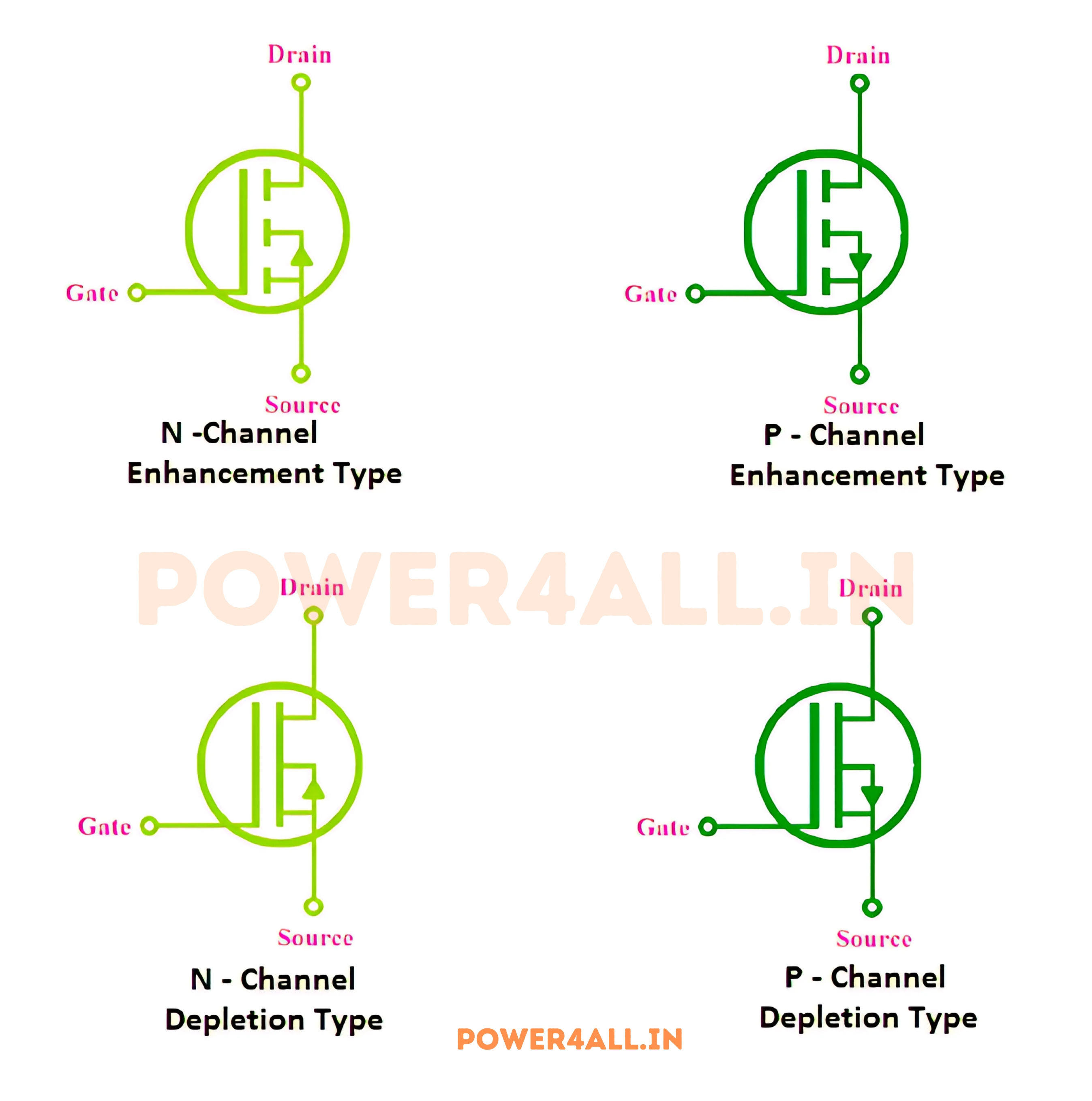
Enhancement Mode MOSFETs
N-Channel Enhancement
Most common MOSFET type
Operating Characteristics
- Normally OFF: No current flows when VGS = 0
- Turn-on: Positive VGS creates electron channel
- Threshold voltage: Typically 1-4V
- Current carriers: Electrons (majority carriers)
- Substrate: P-type silicon
Applications
- Low-side switching in power supplies
- Logic level switching (3.3V, 5V)
- Motor drive circuits
- Digital logic gates
- Power management ICs
VGS > VTH = Channel ON
N-channel enhancement turn-on condition
P-Channel Enhancement
Complementary to N-channel devices
Operating Characteristics
- Normally OFF: No current flows when VGS = 0
- Turn-on: Negative VGS creates hole channel
- Threshold voltage: Typically -1V to -4V
- Current carriers: Holes (majority carriers)
- Substrate: N-type silicon
Applications
- High-side switching applications
- CMOS logic circuits (complementary pair)
- Load switching without level shifters
- Battery protection circuits
- Reverse polarity protection
VGS < VTH = Channel ON
P-channel enhancement turn-on condition
Depletion Mode MOSFETs
Understanding Depletion Mode Operation
Depletion Mode Characteristics
Depletion mode MOSFETs have a pre-existing channel and are normally conducting. They require an opposite polarity gate voltage to reduce or eliminate current flow.
| MOSFET Type | Channel at VGS=0 | Turn-OFF Condition | Typical VTH | Applications |
|---|---|---|---|---|
| N-Channel Depletion | Conducting (ON) | VGS < VTH (negative) | -2V to -6V | Current sources, analog circuits |
| P-Channel Depletion | Conducting (ON) | VGS > VTH (positive) | +2V to +6V | Current sources, load circuits |
Advantages and Disadvantages
Advantages
Always conducting without control signal, useful for current sources, simpler gate drive for some applications.
Disadvantages
Power consumption when OFF is desired, less common and more expensive, requires negative/positive voltage to turn OFF.
MOSFET Type Comparison
| Parameter | N-Ch Enhancement | P-Ch Enhancement | N-Ch Depletion | P-Ch Depletion |
|---|---|---|---|---|
| Default State | OFF | OFF | ON | ON |
| Turn-ON Voltage | Positive VGS | Negative VGS | Default ON | Default ON |
| Turn-OFF Voltage | VGS = 0 | VGS = 0 | Negative VGS | Positive VGS |
| Common Use | Digital switching | High-side switching | Analog circuits | Current sources |
| Availability | Very common | Common | Rare | Very rare |
Selection Guideline
N-channel enhancement MOSFETs are the most common choice for general switching applications due to lower cost, better availability, and superior electrical characteristics. P-channel devices are used when high-side switching or CMOS logic is required.
MOSFET Operating Regions & Modes
MOSFETs operate in three distinct regions depending on the applied voltages. Understanding these operating regions is essential for both analog and digital circuit design, as each region offers different characteristics suitable for specific applications.
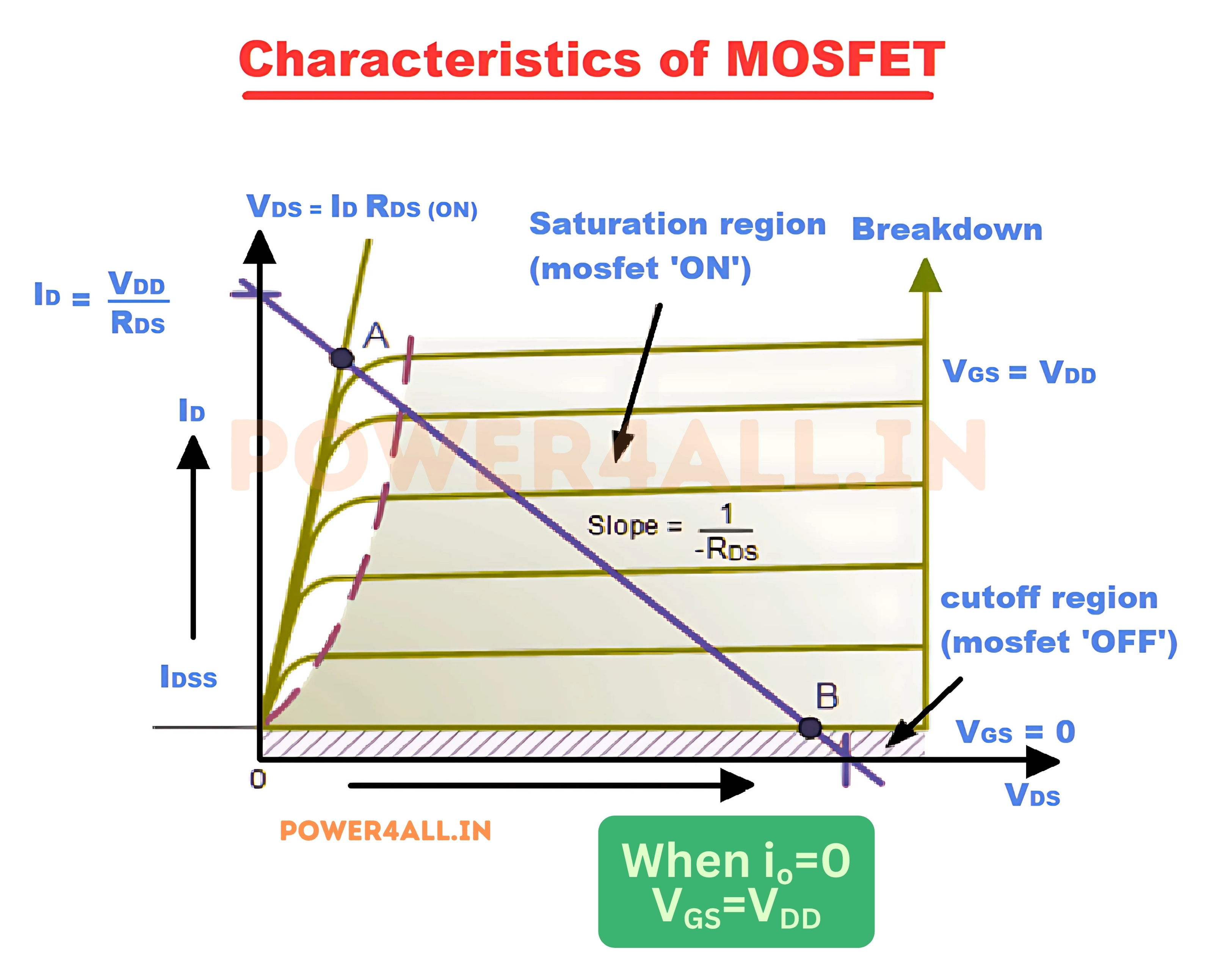
1. Cut-off Region (Sub-threshold)
Non-Conducting State
In the cut-off region, the MOSFET acts as an open switch with virtually no current flowing between drain and source. This occurs when the gate-source voltage is below the threshold voltage.
Key Characteristics
- Condition: VGS < VTH
- Drain current: ID ≈ 0 (only leakage current)
- Channel: No conductive channel formed
- Resistance: RDS = ∞ (open circuit)
- Power dissipation: Minimal (only leakage)
ID ≈ 0 when VGS < VTH
Cut-off region condition
Digital Applications
- Logic '0' state: Represents digital OFF
- Power savings: Minimal static power consumption
- Isolation: Complete electrical isolation
- Standby mode: Low power device operation
2. Triode Region (Linear/Ohmic)
Variable Resistor Operation
MOSFET acts like a voltage-controlled resistor
Operating Conditions
- Gate condition: VGS > VTH
- Drain condition: VDS < (VGS - VTH)
- Channel state: Continuous channel exists
- Current-voltage: Linear relationship
Mathematical Model
ID = μnCox(W/L)[(VGS-VTH)VDS - VDS²/2]
Triode region current equation
Applications
- Analog switches: Signal routing and multiplexing
- Variable resistors: Voltage-controlled attenuation
- Linear amplifiers: Small-signal amplification
- Voltage followers: Buffer circuits
Deep Triode Operation
Low RDS(on) for efficient switching
Low Resistance State
- Condition: VGS >> VTH and VDS is small
- Resistance: RDS(on) = 1/[μnCox(W/L)(VGS-VTH)]
- Power loss: PD = ID² × RDS(on)
- Heat generation: I²R losses in the channel
Design Considerations
- Gate overdrive: Use VGS well above VTH
- W/L ratio: Wide, short channels for low RDS(on)
- Thermal management: Heat sinking for power applications
- Gate drive: Sufficient current for fast switching
Typical RDS(on) Values
- Small signal: 1-100Ω
- Medium power: 10-100mΩ
- High power: 1-10mΩ
- Ultra-low RDS(on): <1mΩ
3. Saturation Region (Active)
Constant Current Source Operation
Saturation Region Characteristics
In saturation, the MOSFET operates as a voltage-controlled current source. The drain current becomes independent of drain-source voltage and depends primarily on gate-source voltage.
Operating Conditions
VGS > VTH and VDS > (VGS - VTH). Channel pinches off near the drain, creating constant current behavior.
Current Equation
ID = (μnCox/2)(W/L)(VGS - VTH)². Current is proportional to the square of gate overdrive voltage.
Transconductance
gm = ∂ID/∂VGS = μnCox(W/L)(VGS - VTH). Determines amplification capability.
Output Resistance
ro = ∂VDS/∂ID ≈ 1/(λID). High output resistance makes it ideal for current sources.
Applications in Saturation
| Application | Circuit Type | Key Advantage | Design Focus |
|---|---|---|---|
| Voltage Amplifiers | Common source, common gate | High voltage gain | Maximize gm and ro |
| Current Sources | Current mirrors, bias circuits | Constant current output | High output resistance |
| Differential Pairs | Op-amp input stages | High CMRR, low offset | Device matching |
| Oscillators | LC, crystal oscillators | Negative resistance | Phase and gain control |
Av = -gm × ro
Voltage gain in saturation region
Region Selection for Applications
Digital Switching
Cut-off and Triode regions
- OFF state: Cut-off region (VGS < VTH)
- ON state: Deep triode (VGS >> VTH)
- Advantages: Low power, fast switching
- Applications: Logic gates, processors, memory
Analog Amplification
Saturation region operation
- Bias point: Saturation region
- Signal swing: Stay within saturation
- Advantages: High gain, linearity
- Applications: Op-amps, RF amplifiers
Design Tip
For switching applications, design the circuit to operate in cut-off (OFF) and deep triode (ON) regions. For amplification, bias the MOSFET in saturation and ensure small signal operation doesn't push it into triode region.
MOSFET as an Electronic Switch
MOSFETs excel as electronic switches due to their fast switching speeds, low on-resistance, high input impedance, and voltage control operation. They have largely replaced bipolar transistors in most switching applications due to superior efficiency and ease of control.
Switching Operation Fundamentals
Perfect Switch Characteristics
An ideal switch has zero resistance when ON and infinite resistance when OFF, with instantaneous switching. MOSFETs approach this ideal better than any other switching device.
MOSFET Switch States
- OFF state: VGS < VTH, RDS = ∞, ID = 0
- ON state: VGS > VTH, RDS = RDS(on), ID = VDD/RLoad
- Transition time: Typically 10-100 nanoseconds
- Control power: Virtually zero static power
Switch Performance Metrics
- RDS(on): 1mΩ - 1Ω (on-resistance)
- Switch time: 1ns - 1μs
- Gate charge: 1nC - 1000nC
- Breakdown voltage: 20V - 1000V+
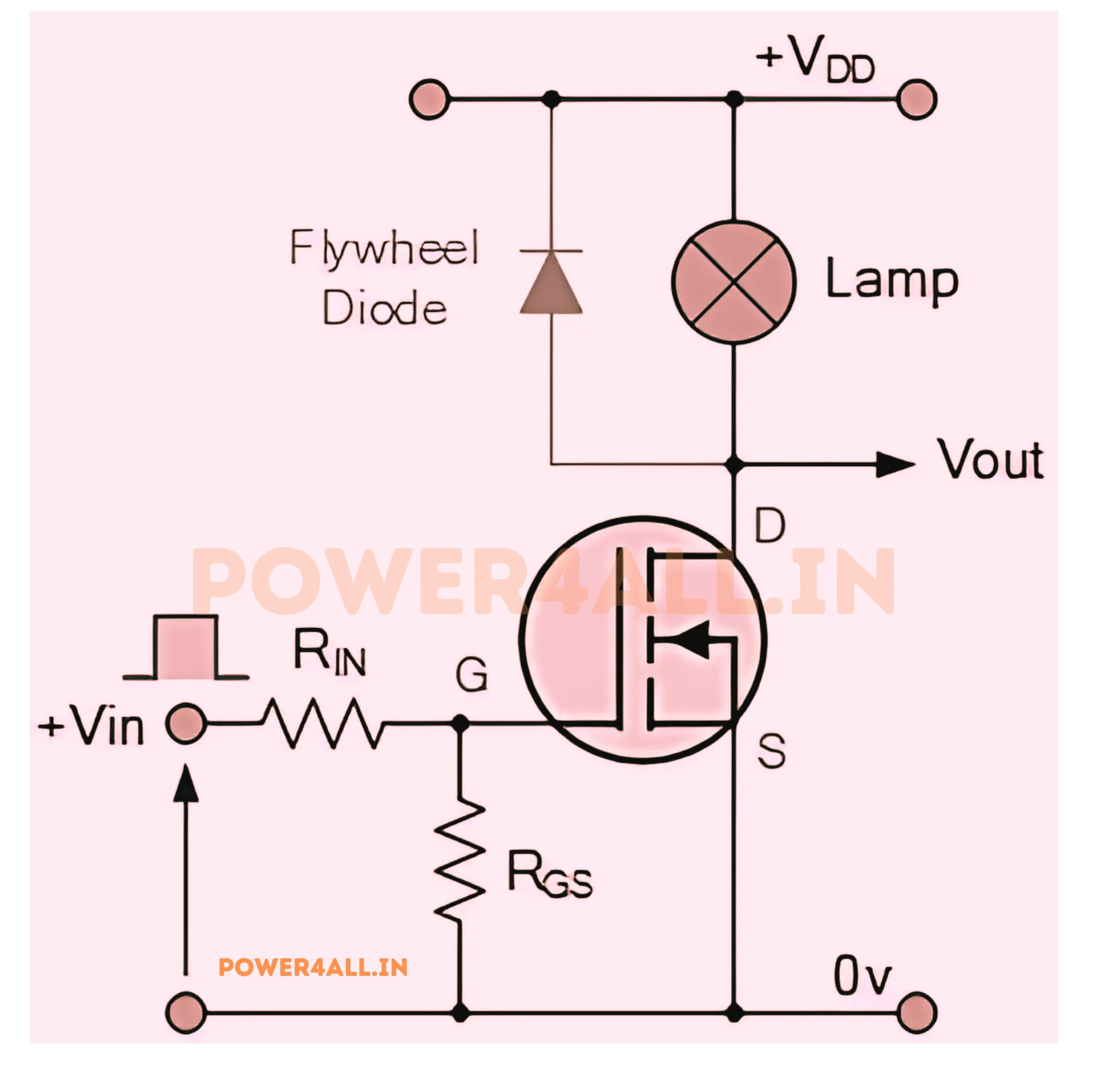
Low-Side vs High-Side Switching
Low-Side Switching
MOSFET connects load to ground
Circuit Configuration
- MOSFET position: Between load and ground
- Load connection: Between VDD and MOSFET drain
- Gate drive: Simple, referenced to ground
- Source connection: Connected to ground (0V)
Advantages
- Simple gate drive: No level shifting required
- Lower cost: N-channel MOSFETs preferred
- Better performance: N-channel has lower RDS(on)
- Easy control: Direct microcontroller interface
Disadvantages
- Load not isolated: Load floats above ground when OFF
- Ground current: All load current flows through switch
- EMI considerations: Fast switching of ground current
High-Side Switching
MOSFET connects VDD to load
Circuit Configuration
- MOSFET position: Between VDD and load
- Load connection: Between MOSFET source and ground
- Gate drive: Requires level shifting or P-channel
- Source voltage: Follows VDD voltage
Advantages
- Ground isolation: Load has solid ground connection
- Better EMI: VDD rail switching instead of ground
- Protection: Easier current sensing and protection
- Safety: Load disconnected from power when OFF
Implementation Options
- P-channel MOSFET: Simple drive, higher RDS(on)
- N-channel + bootstrap: Better performance, complex drive
- Gate driver IC: Integrated solution with level shifting
- Charge pump: Generate higher gate voltage
Switching Speed and Timing
Understanding MOSFET Switching Transitions
Switching Waveforms and Timing
MOSFET switching involves several distinct phases, each limited by different capacitances and resistances in the circuit.
| Switching Phase | Duration | Limiting Factor | Description |
|---|---|---|---|
| Turn-on Delay (td(on)) | 5-50ns | CGS charging | Gate voltage rises from 0V to VTH |
| Current Rise (tr) | 10-100ns | CGS charging | Drain current rises from 0 to full load current |
| Voltage Fall (tf) | 20-200ns | CGD (Miller) | Drain voltage falls, Miller effect dominates |
| Turn-off Delay (td(off)) | 10-100ns | Gate discharge | Gate voltage falls from VGS to VTH |
Miller Effect and CGD
Miller Capacitance
CGD appears as (1 + Av) × CGD at the gate due to voltage amplification, significantly slowing switching transitions.
Miller Plateau
Gate voltage plateaus during drain voltage transition due to Miller feedback, creating constant current charging period.
Fast Switching
Low gate resistance and high gate current capability reduce switching times and minimize switching losses.
tsw ≈ RG × (CGS + CGD × (1 + gm × RLoad))
Approximate switching time with Miller effect
Gate Drive Circuits
Direct Drive
Simple microcontroller or logic gate drive
Circuit Elements
- Gate resistor: Limits inrush current, controls switching speed
- Pull-down resistor: Ensures OFF state when not driven
- Protection diode: Clamps negative voltage transients
- Logic interface: 3.3V or 5V logic compatibility
Design Considerations
- Gate resistor value: 10-1000Ω typical
- Pull-down resistor: 10kΩ typical
- Drive capability: Output current of driving device
- Logic threshold: VTH vs. logic levels
Gate Driver ICs
Dedicated high-performance gate drivers
Features
- High peak current: 1A-10A gate drive capability
- Fast switching: Propagation delays <50ns
- Level shifting: High-side and low-side drive
- Protection: UVLO, thermal shutdown
Popular Gate Drivers
- IR2110: High/low side driver, 500V rating
- UCC27201: 120V half-bridge driver
- SI8271: Isolated gate driver
- LTC4440: High-speed, high-voltage driver
Gate Driver Selection
- Peak current: QG / desired switching time
- Voltage rating: Match or exceed MOSFET VGS
- Propagation delay: Critical for high-frequency switching
- Package and thermal: Power dissipation considerations
Gate Drive Guidelines
Always use appropriate gate drive voltage (typically 10-15V for power MOSFETs), include gate resistors to control di/dt and reduce EMI, ensure fast turn-off to minimize switching losses, and protect against gate voltage exceeding maximum ratings.
MOSFET vs BJT vs SCR Comparison
Understanding the differences between MOSFETs, BJTs (Bipolar Junction Transistors), and SCRs (Silicon Controlled Rectifiers) is crucial for selecting the right device for specific applications. Each has unique advantages and optimal use cases.
Comprehensive Device Comparison
| Parameter | MOSFET | BJT | SCR |
|---|---|---|---|
| Control Type | Voltage controlled | Current controlled | Current triggered |
| Input Impedance | Very high (10¹⁴Ω) | Low to medium (1kΩ-100kΩ) | Low (during trigger) |
| Switching Speed | Very fast (ns) | Fast (ns-μs) | Medium (μs) |
| Power Consumption | Very low | Medium | High (when conducting) |
| Terminals | Gate, Source, Drain | Base, Emitter, Collector | Gate, Anode, Cathode |
| Charge Carriers | Unipolar (electrons or holes) | Bipolar (electrons and holes) | Bipolar (electrons and holes) |
| Temperature Stability | Good (positive tempco) | Poor (negative tempco) | Good (positive tempco) |
| Voltage Drop (ON) | ID × RDS(on) | VCE(sat) ≈ 0.2V | VF ≈ 1-2V |
| Turn-off Method | Remove gate voltage | Remove base current | Current must go to zero |
| Maximum Frequency | MHz to GHz | MHz | Hz to kHz |
Application-Specific Comparisons
Digital Logic & Processing
MOSFETs dominate digital applications
Why MOSFETs Win
- Ultra-low power: Essential for battery devices and high integration
- High integration: Billions of transistors possible
- Fast switching: GHz operation capabilities
- Voltage control: Easy interfacing with digital signals
- Scalability: Technology scales to nanometer dimensions
Applications
- Microprocessors and microcontrollers
- Memory devices (RAM, Flash, SSD)
- Digital signal processors (DSP)
- FPGA and ASIC designs
- Mobile device processors
Modern Processor Stats
- Transistor count: >50 billion MOSFETs
- Feature size: 3-7nm technology
- Clock speed: 3-5GHz
- Power efficiency: <1W per billion transistors
Analog & RF Applications
Mixed preference based on frequency and requirements
MOSFET Advantages
- High input impedance: Minimal loading of signal sources
- Low noise: Better for sensitive RF applications
- High frequency: GHz operation possible
- Low power: Battery-powered applications
BJT Advantages
- High transconductance: Better voltage gain
- Lower 1/f noise: Better at low frequencies
- Better matching: More predictable parameters
- Linear operation: Excellent for analog circuits
Application Selection
- RF amplifiers: MOSFETs preferred above 1GHz
- Audio amplifiers: BJTs preferred for linearity
- Op-amps: Both used, design dependent
- Oscillators: Both used, frequency dependent
Power Electronics
Device selection depends on power level and frequency
MOSFET Dominance
- Switching power supplies: Up to 1MHz+ switching
- Motor drives: Up to 100kW systems
- DC-DC converters: High efficiency critical
- LED drivers: Precise current control
BJT Applications
- Linear regulators: Low dropout applications
- Audio power: Class AB amplifiers
- Low cost switching: Simple on/off control
SCR Applications
- AC power control: Phase control, soft starters
- High power: >100A applications
- Line frequency: 50/60Hz applications
- Crowbar protection: Overvoltage protection
MOSFET Applications & Real-World Uses
MOSFETs are ubiquitous in modern electronics, from the billions of transistors in your smartphone processor to the power switches in electric vehicles. Their versatility, efficiency, and scalability make them essential components across virtually every electronic application.
Digital Electronics Applications
Microprocessors & Logic
The foundation of digital computing
Key Applications
- CPU cores: Billions of MOSFETs in modern processors
- Logic gates: NAND, NOR, NOT, and complex logic functions
- Cache memory: SRAM cells using 6 MOSFETs per bit
- GPU processors: Thousands of parallel processing cores
- Microcontrollers: Embedded control systems
Technical Implementation
- CMOS technology: Complementary N and P-channel pairs
- Feature sizes: 3nm to 180nm technology nodes
- Power scaling: Voltage scaling from 5V to 1V and below
- Speed optimization: Multi-GHz operation capabilities
Modern Processor Examples
- Apple M1 Ultra: 114 billion transistors, 5nm process
- AMD Ryzen 9: 19.2 billion transistors, 7nm process
- Intel Core i9: 17.7 billion transistors, 10nm process
- Mobile processors: 15+ billion transistors in smartphones
Memory Technologies
Data storage and retrieval systems
Memory Types
- DRAM: Dynamic RAM using 1 MOSFET + 1 capacitor per bit
- SRAM: Static RAM using 6 MOSFETs per bit
- Flash memory: Non-volatile storage in SSDs and USB drives
- EEPROM: Electrically erasable programmable memory
- ROM: Read-only memory for firmware storage
Advanced Memory
- 3D NAND: Stacked flash memory for high density
- DDR5 RAM: High-speed system memory
- HBM memory: High bandwidth memory for GPUs
- Embedded memory: On-chip cache and storage
Density = 2^n bits per chip
Memory scaling with technology advancement
Power Electronics Applications
Switching Power Supplies
MOSFETs are the heart of modern power supplies, enabling high efficiency and compact designs through fast switching operation.
Power Supply Types
- Buck converters: Step-down DC-DC conversion
- Boost converters: Step-up DC-DC conversion
- Buck-boost: Step-up or step-down capability
- Flyback: Isolated power conversion
- Forward: Transformer-based isolation
- LLC resonant: High-efficiency soft switching
Power Supply Specifications
- Efficiency: 85-98% typical
- Switching frequency: 50kHz - 2MHz
- Power levels: mW to MW
- Size reduction: 50-90% vs linear supplies
Motor Drive and Control Systems
Electric Motor Control
Precision speed and torque control
Motor Types Controlled
- BLDC motors: Brushless DC motor drives
- AC induction: Variable frequency drives (VFD)
- Stepper motors: Precision positioning systems
- Servo motors: High-performance feedback control
- Linear motors: Direct linear motion control
Control Techniques
- PWM control: Pulse width modulation for speed
- Vector control: Field-oriented control (FOC)
- Six-step control: Simple commutation for BLDC
- Sinusoidal control: Smooth operation with low ripple
Automotive Applications
- Electric vehicles: Traction motor inverters (200kW+)
- Power steering: Electric power assist systems
- HVAC blowers: Variable speed fan control
- Window motors: Precise positioning control
Power Inverters
DC to AC power conversion
Inverter Applications
- Solar inverters: Grid-tie and off-grid systems
- UPS systems: Uninterruptible power supplies
- Motor drives: Variable frequency drives
- Welding machines: High-frequency arc welding
- Induction heating: High-frequency heating systems
Inverter Topologies
- Single-phase: Residential and light commercial
- Three-phase: Industrial and high-power systems
- Multilevel: High voltage, low harmonic distortion
- Resonant: Soft switching for high efficiency
Performance Metrics
- Efficiency: 95-98% for modern designs
- THD: <3% for grid-tie applications
- Switching frequency: 10-100kHz typical
- Power factor: >0.99 with active PFC
Consumer Electronics
MOSFETs in Everyday Consumer Devices
Smartphone and Mobile Devices
| Component | MOSFET Function | Key Requirements |
|---|---|---|
| Application Processor | Logic gates, memory interfaces | Ultra-low power, high speed |
| Power Management IC | DC-DC converters, LDOs | High efficiency, small size |
| Audio Amplifier | Class-D switching amplifiers | Low distortion, high efficiency |
| Display Driver | Backlight control, pixel drivers | Precise current control |
| Charging Circuit | Battery protection, power switching | Safety, efficiency |
Home Appliances
Kitchen Appliances
Microwave ovens (magnetron power supply), induction cooktops (high-frequency inverters), dishwashers (motor control), refrigerators (compressor drives).
Entertainment Systems
TV power supplies and backlighting, audio amplifiers, gaming consoles, streaming devices, smart speakers with voice processing.
Lighting Systems
LED driver circuits, smart bulbs with wireless control, dimmable lighting systems, emergency lighting with battery backup.
HVAC Systems
Variable speed fan drives, heat pump compressor control, smart thermostats, air quality monitoring systems.
Computing and IT Equipment
Data Center and Server Applications
- Server processors: Multi-core CPUs with billions of MOSFETs
- Memory modules: DDR4/DDR5 RAM with error correction
- Storage systems: SSD controllers and NAND flash memory
- Network equipment: Switch ASICs and PHY interfaces
- Power distribution: 48V to point-of-load converters
- Cooling systems: Variable speed fans and pumps
Automotive Electronics
Electric Vehicle Systems
High-power automotive applications
Powertrain Components
- Traction inverter: 50-400kW motor drive systems
- DC-DC converter: 400V to 12V conversion
- Onboard charger: AC to DC battery charging
- Battery management: Cell balancing and protection
- Auxiliary drives: Compressor, heater, pumps
Technical Challenges
- High temperature: Operation up to 175°C
- Vibration resistance: Automotive environmental stress
- EMI/EMC: Electromagnetic compatibility requirements
- Functional safety: ASIL-D safety requirements
- Efficiency: >98% for maximum range
Traditional Automotive
Internal combustion engine vehicles
Engine Management
- Fuel injection: Precise injector timing control
- Ignition systems: Coil-on-plug ignition drives
- Throttle control: Electronic throttle body
- Turbocharger: Wastegate and VGT control
- Emissions control: SCR, DPF, and catalyst heating
Body Electronics
- Power windows: Motor drive and anti-pinch
- Seat adjustment: Multi-motor position control
- Lighting systems: LED headlights and adaptive lighting
- HVAC control: Blower speed and temperature control
- Infotainment: Audio amplifiers and display drivers
Industrial and Renewable Energy
Solar Energy Systems
Photovoltaic power conversion
System Components
- String inverters: 1-100kW centralized conversion
- Power optimizers: Panel-level MPPT tracking
- Microinverters: Individual panel AC conversion
- Energy storage: Battery charge/discharge control
- Grid management: Smart grid interface systems
Performance Requirements
- Efficiency: >98% for utility-scale systems
- Reliability: 25+ year operational life
- Grid compliance: IEEE 1547 and utility standards
- Safety: Rapid shutdown and arc fault protection
Wind Energy Systems
Wind turbine power conversion
Wind Turbine Electronics
- Generator-side converter: Variable speed control
- Grid-side converter: Power factor correction
- Pitch control: Blade angle optimization
- Yaw control: Turbine orientation system
- Protection systems: Fault ride-through capability
Industrial Automation
- Factory automation: Motor drives and robotics
- Process control: Temperature and flow control
- Material handling: Conveyor and crane systems
- Machine tools: CNC and precision positioning
Market Growth
The global MOSFET market is expected to reach $12+ billion by 2028, driven by electric vehicles, renewable energy, 5G infrastructure, and IoT devices. Power MOSFETs represent the fastest-growing segment due to electrification trends.
MOSFET Selection & Design Guide
Proper MOSFET selection is critical for circuit performance, efficiency, and reliability. This comprehensive guide covers the key parameters, trade-offs, and design considerations needed to choose the optimal MOSFET for any application.
Key MOSFET Parameters
| Parameter | Symbol | Importance | Design Impact | Typical Range |
|---|---|---|---|---|
| Drain-Source Voltage | VDS(max) | Critical | Determines voltage rating | 20V - 1700V |
| Continuous Drain Current | ID(max) | Critical | Current handling capability | 100mA - 500A |
| On-Resistance | RDS(on) | High | Conduction losses | 1mΩ - 10Ω |
| Threshold Voltage | VTH | High | Gate drive compatibility | 0.5V - 4V |
| Gate Charge | QG | Medium | Switching speed, drive power | 1nC - 1000nC |
| Input Capacitance | CISS | Medium | Switching speed | 100pF - 10nF |
| Thermal Resistance | RθJC | High | Thermal design | 0.1°C/W - 100°C/W |
Voltage Rating Selection
Voltage Derating Guidelines
Always derate MOSFET voltage ratings to account for transients and safety margins. Operating too close to maximum ratings reduces reliability and increases failure risk.
Derating Factors
- Continuous operation: Use 80% of VDS(max)
- Switching applications: Use 70% of VDS(max)
- Automotive/harsh environment: Use 60% of VDS(max)
- High reliability: Use 50% of VDS(max)
Voltage Selection Example
48V system with ±20% variation:
- Maximum system voltage: 48V × 1.2 = 57.6V
- Transient spikes: Add 50% margin = 86.4V
- Safety derating: 86.4V ÷ 0.8 = 108V
- Selected MOSFET: 150V rating
- Actual margin: 150V ÷ 86.4V = 74% margin
VDS(rated) ≥ VDS(max) ÷ Derating Factor
Voltage rating selection formula
Current Rating and Thermal Design
Current Handling and Heat Management
Current Rating Considerations
MOSFET current rating depends on thermal design, switching frequency, and ambient temperature. The maximum current is typically limited by junction temperature, not device physics.
Thermal Limitations
Current rating decreases with temperature. At 25°C case temperature, full current is available. At 100°C case temperature, current may be derated to 50-70%.
RDS(on) Impact
Power dissipation PD = I²RDS(on). Lower RDS(on) allows higher current for same power dissipation. RDS(on) increases ~70% from 25°C to 125°C.
Switching Losses
At high switching frequencies, switching losses may exceed conduction losses. Total loss = conduction loss + switching loss.
Thermal Design Process
Thermal Design Example
30A continuous current, 100V MOSFET:
- RDS(on) @ 25°C: 5mΩ
- RDS(on) @ 125°C: 8.5mΩ (70% increase)
- Power dissipation: 30² × 8.5mΩ = 7.65W
- RθJC: 1.5°C/W (TO-247 package)
- Required RθSA: (150°C - 70°C)/7.65W - 1.5°C/W = 8.95°C/W
- Heat sink selection: Choose RθSA ≤ 8°C/W
Switching Performance Optimization
Gate Drive Design
Optimizing switching speed and efficiency
Gate Drive Parameters
- Gate voltage: 10-15V for power MOSFETs
- Gate current: QG / switching time target
- Gate resistance: Balance speed vs. EMI
- Dead time: Prevent shoot-through in bridges
Drive Circuit Options
- Direct drive: Microcontroller or logic output
- Buffer amplifiers: Discrete transistor drivers
- Gate driver ICs: Dedicated high-performance drivers
- Isolated drivers: Galvanic isolation for safety
IGate = QG / tswitch
Required gate current for target switching time
Switching Loss Calculation
Minimizing switching power losses
Loss Components
- Turn-on loss: Eon = ½ × V × I × ton
- Turn-off loss: Eoff = ½ × V × I × toff
- Gate drive loss: PGate = QG × VGate × fsw
- Dead time loss: Body diode conduction
Loss Reduction Techniques
- Fast switching: Low RG, high gate current
- Soft switching: ZVS/ZCS resonant circuits
- Synchronous rectification: Replace diodes with MOSFETs
- Optimal frequency: Balance switching vs. conduction losses
High-Frequency Considerations
- Parasitic inductance: Minimize loop inductance
- Gate ringing: Ferrite beads, RC snubbers
- PCB layout: Low inductance, proper grounding
- EMI management: Shielding, filtering
Application-Specific Selection Guide
| Application | Key Parameters | Typical Ratings | Special Considerations |
|---|---|---|---|
| Power Supplies | Low RDS(on), fast switching | 30-200V, 1-100A | Low gate charge, avalanche rating |
| Motor Drives | High current, ruggedness | 600-1200V, 10-500A | Short circuit protection, avalanche |
| Electric Vehicles | Ultra-low losses, reliability | 650-1200V, 100-1000A | Automotive qualification, thermal cycling |
| Solar Inverters | High efficiency, long life | 600-1500V, 20-200A | 25+ year reliability, grid standards |
| LED Drivers | Logic level, low cost | 30-100V, 1-10A | PWM dimming capability |
| Battery Protection | Low RDS(on), small size | 20-60V, 1-100A | Back-to-back configuration |
Advanced MOSFET Technologies
Silicon Carbide (SiC)
Wide bandgap technology for extreme performance
Advantages
- Higher voltage: Up to 3300V in single device
- Higher temperature: 200°C junction temperature
- Lower losses: 90% reduction vs. silicon
- Higher frequency: >100kHz switching
- Smaller size: Reduced passive components
Applications
- Electric vehicle traction inverters
- Solar inverters and energy storage
- Industrial motor drives
- Power factor correction
- High-voltage DC transmission
Design Considerations
- Gate drive: -5V to +20V recommended
- Higher cost: 5-10× vs. silicon
- Gate protection: More sensitive to overvoltage
- PCB design: Fast switching requires careful layout
Gallium Nitride (GaN)
Ultra-high frequency and efficiency
Advantages
- Ultra-fast switching: <10ns transitions
- Very low losses: Minimal switching losses
- High frequency: MHz switching capability
- Compact size: Very small packages
- Zero reverse recovery: No body diode issues
Applications
- USB-C and laptop chargers
- Wireless charging systems
- Envelope tracking for 5G
- LiDAR and radar systems
- High-frequency power supplies
Limitations
- Voltage limitation: Typically <650V
- Current limitation: Lower than silicon
- Cost: Higher than silicon, less than SiC
- Gate drive: 0V to +6V operation
Selection Summary
Start with application requirements (voltage, current, frequency), calculate power losses and thermal requirements, consider cost and availability constraints, and prototype with selected devices to verify performance. Always include adequate safety margins and consider worst-case operating conditions.
MOSFET Testing & Troubleshooting
Proper testing and troubleshooting techniques are essential for MOSFET circuit development and maintenance. Understanding common failure modes, measurement techniques, and diagnostic procedures enables quick problem resolution and reliable circuit operation.
Basic MOSFET Testing with Multimeter
Diode Test Method
Simple go/no-go testing using multimeter diode mode
Test Procedure
Expected Results
- Good MOSFET: Body diode forward = 0.6-0.8V, reverse = OL
- Gate isolation: >10MΩ resistance to source and drain
- Failed MOSFET: Short circuit or open circuit readings
Dynamic Testing
Testing MOSFET switching behavior
Simple Switch Test
- Test circuit: 12V supply, 1kΩ load resistor, MOSFET
- Gate drive: 0V to 10V signal applied to gate
- Expected behavior: Load current ON/OFF with gate signal
- Measurements: Drain voltage should switch between 0V and VDD
Gate Threshold Test
- Setup: Variable voltage source connected to gate
- Measurement: Monitor drain current vs. gate voltage
- Threshold voltage: VGS where drain current begins to flow
- Typical values: 1-4V for most MOSFETs
Test Equipment Needed
- Digital multimeter: With diode test function
- Variable power supply: 0-15V adjustable
- Oscilloscope: For dynamic testing
- Function generator: For switching speed tests
- Load resistors: Various values for testing
Advanced Testing Techniques
Curve Tracer and Parametric Testing
Curve Tracer Measurements
Curve tracers provide comprehensive MOSFET characterization by plotting I-V curves under various gate voltages and measuring key parameters.
| Parameter | Test Method | Expected Range | Failure Indicators |
|---|---|---|---|
| VTH (Threshold Voltage) | ID vs VGS at constant VDS | 1-4V typical | Outside datasheet limits |
| RDS(on) | VDS/ID in linear region | mΩ to Ω range | Significantly higher than spec |
| IDSS (Leakage) | ID at VGS=0, high VDS | nA to μA range | Excessive leakage current |
| Transconductance | ∂ID/∂VGS in saturation | mS to S range | Lower than expected |
| Breakdown Voltage | VDS at specified ID | Per datasheet rating | Early breakdown |
High-Frequency Testing
Switching Speed
Use fast oscilloscope to measure turn-on/turn-off times. Rise time should match datasheet specifications under similar conditions.
Gate Charge
Measure gate charge (QG) using constant current source. Plot VGS vs time to determine total gate charge and Miller plateau.
Capacitance
Use LCR meter or network analyzer to measure CISS, COSS, and CRSS at different voltages and frequencies.
Common MOSFET Failure Modes
Gate Oxide Breakdown
Most common MOSFET failure
Causes
- ESD damage: Electrostatic discharge during handling
- Overvoltage: Gate voltage exceeding maximum rating
- Transients: Fast voltage spikes from switching
- Manufacturing defects: Thin or contaminated oxide
Symptoms
- Gate-source short: Low resistance between gate and source
- High leakage: Excessive gate current
- No control: Gate has no effect on drain current
- Permanent conduction: Always ON regardless of gate voltage
Prevention
- ESD protection: Proper grounding and handling procedures
- Gate protection: Zener diodes or TVS diodes
- Voltage limiting: Never exceed VGS(max) rating
- Slow switching: Gate resistors to limit dv/dt
Thermal Failure
Overheating and thermal damage
Causes
- Inadequate cooling: Insufficient heat sinking
- Overcurrent: Current exceeding safe operating area
- High switching losses: Poor gate drive or high frequency
- Thermal cycling: Repeated temperature changes
Symptoms
- Increased RDS(on): Higher resistance when ON
- Parameter drift: Threshold voltage changes
- Physical damage: Burnt package or bond wires
- Intermittent operation: Works when cool, fails when hot
Prevention
- Proper heat sinking: Adequate thermal management
- Current derating: Stay within SOA limits
- Switching optimization: Fast, clean switching
- Thermal monitoring: Temperature sensors and protection
Troubleshooting Procedures
| Problem | Symptoms | Possible Causes | Troubleshooting Steps |
|---|---|---|---|
| MOSFET Won't Turn ON | No drain current, high drain voltage | Insufficient gate drive, failed gate, open circuit | Check gate voltage, verify gate drive circuit, test MOSFET |
| MOSFET Won't Turn OFF | Continuous drain current | Gate drive not reaching zero, gate short, thermal runaway | Check gate-source voltage, verify gate drive, check temperature |
| High RDS(on) | Excessive voltage drop when ON | Insufficient gate drive, partial gate failure, heating | Measure gate voltage, check for proper gate drive, verify cooling |
| Slow Switching | Long rise/fall times, high switching losses | High gate resistance, poor PCB layout, capacitive loading | Reduce gate resistance, improve layout, check gate drive current |
| Oscillation | Ringing on gate or drain, EMI issues | Parasitic inductance, poor layout, insufficient damping | Add gate resistor, improve PCB layout, use snubbers |
Safety During Testing
Always discharge gate capacitance before handling MOSFETs. Use ESD protection when testing. Be aware that gate oxide is extremely thin and easily damaged. Power off circuits completely before making connections or measuring resistance.
MOSFET Safety Considerations
Working with MOSFETs requires attention to both electrical and thermal safety. The extremely thin gate oxide makes MOSFETs particularly sensitive to electrostatic discharge, while power MOSFETs can generate significant heat requiring proper thermal management and safety precautions.
Electrostatic Discharge (ESD) Protection
ESD Sensitivity
MOSFETs are among the most ESD-sensitive components in electronics. The gate oxide layer is typically only 1-10 nanometers thick, making it vulnerable to damage from static electricity that can easily reach thousands of volts.
ESD Damage Mechanisms
- Gate oxide puncture: Permanent breakdown of insulating layer
- Metal migration: High current causes metal traces to move
- Junction damage: Secondary breakdown in source/drain regions
- Latent damage: Weakened oxide fails later under stress
ESD Voltage Levels
- Human body: Up to 25,000V
- Carpet walking: 1,500-35,000V
- Plastic movement: 1,000-20,000V
- MOSFET damage: As low as 30-100V
ESD Protection Measures
- Grounded work area: ESD mat and wrist strap
- Conductive packaging: Antistatic bags and foam
- Ionized air: Neutralize static charges
- Humidity control: 40-60% relative humidity
- ESD-safe tools: Grounded soldering irons
Electrical Safety
Voltage and Current Safety
Protection against electrical hazards
High Voltage Precautions
- Gate voltage limits: Never exceed VGS(max) rating
- Drain voltage safety: Respect VDS breakdown voltage
- Isolation: Proper isolation for high-voltage circuits
- Discharge procedures: Safely discharge capacitors
Current Protection
- Safe operating area: Stay within SOA limits
- Current limiting: Fuses or current limiting resistors
- Short circuit protection: Fast-acting protection circuits
- Overcurrent detection: Current sensing and shutdown
P = V × I (within SOA)
Power must stay within safe operating area
Gate Drive Safety
Safe gate drive circuit design
Protection Circuits
- Gate resistors: Limit current and reduce ringing
- Zener diodes: Clamp gate voltage to safe levels
- TVS diodes: Fast transient voltage suppression
- Ferrite beads: Reduce high-frequency noise
Drive Circuit Guidelines
- Positive and negative drive: Ensure complete turn-off
- Isolated drives: Prevent ground loops
- Fault protection: Shutdown on overcurrent or overtemperature
- Dead time: Prevent shoot-through in bridge circuits
Gate Protection Network
- Series resistor: 10-100Ω typical
- Gate-source resistor: 10kΩ pull-down
- Zener diode: 15-18V rating typical
- Ferrite bead: Reduce HF coupling
Thermal Safety
Heat Management and Burn Prevention
Thermal Hazards
Power MOSFETs can reach temperatures exceeding 150°C during normal operation. Heat sinks and power components can cause burns and present fire hazards if not properly managed.
Hot Surface Protection
Heat sinks and power devices can reach burn-causing temperatures. Use warning labels and protective covers in accessible areas.
Fire Prevention
Overheated components can ignite nearby materials. Ensure adequate clearance and use flame-retardant materials.
Temperature Monitoring
Include thermal sensors and protection circuits to prevent overheating. Monitor junction temperature, not just case temperature.
Thermal Protection Methods
| Protection Method | Implementation | Response Time | Applications |
|---|---|---|---|
| Thermal Fuses | One-time protection device | Seconds | Catastrophic overheating |
| Thermal Switches | Resettable temperature switch | Seconds | Equipment protection |
| Thermistors | Temperature-dependent resistor | Milliseconds | Continuous monitoring |
| IC Temperature Sensors | Digital temperature monitoring | Milliseconds | Precise control systems |
Thermal Safety Guidelines
Never touch heat sinks or power devices during operation. Allow adequate cooling time before handling. Use thermal protection in all power circuits. Provide warning labels for hot surfaces accessible to users.
Circuit Design Safety
Safe PCB Design
Layout considerations for safety and reliability
High Voltage Spacing
- Creepage distance: Minimum distance across PCB surface
- Clearance distance: Minimum air gap distance
- Via placement: Avoid vias near high voltage traces
- Solder mask: Adequate coverage for insulation
Current Handling
- Trace width: Adequate for current without overheating
- Via current: Multiple vias for high current paths
- Thermal vias: Heat dissipation from power devices
- Copper pour: Large areas for heat spreading
System Safety Features
Comprehensive safety systems
Protection Hierarchy
- Primary protection: Proper design and component selection
- Secondary protection: Fuses, circuit breakers, protection ICs
- Tertiary protection: System monitoring and shutdown
- Emergency stops: Manual safety shutoff capability
Fault Response
- Fail-safe design: Safe state when faults occur
- Fault indication: LEDs or displays showing status
- Automatic recovery: System restart after fault clearing
- Maintenance mode: Safe configuration for servicing
Safety Checklist
- ESD protection: All assembly and test procedures
- Thermal management: Adequate cooling for all conditions
- Electrical isolation: Proper safety barriers
- Protection circuits: Multiple levels of protection
- Documentation: Clear safety warnings and procedures
Frequently Asked Questions about MOSFETs
Common questions and comprehensive answers about MOSFET operation, selection, application, and troubleshooting. These FAQs address the most frequent concerns from engineers, students, and hobbyists working with MOSFETs.
Basic MOSFET Questions
What is the difference between a MOSFET and a regular transistor?
MOSFETs and bipolar junction transistors (BJTs) are both transistors but work on different principles:
| Characteristic | MOSFET | BJT |
|---|---|---|
| Control method | Voltage controlled (gate voltage) | Current controlled (base current) |
| Input impedance | Very high (>10¹²Ω) | Medium (1kΩ-100kΩ) |
| Power consumption | Very low (no steady gate current) | Higher (requires base current) |
| Switching speed | Very fast (ns range) | Fast (ns to μs range) |
| Charge carriers | Unipolar (electrons OR holes) | Bipolar (electrons AND holes) |
Key advantage: MOSFETs require virtually no input current, making them ideal for high-efficiency switching and high-input-impedance amplifiers.
What's the difference between enhancement and depletion mode MOSFETs?
Enhancement Mode (Most Common)
- Default state: OFF (no channel exists)
- Turn-on: Requires gate voltage above threshold
- Channel formation: Gate voltage "enhances" or creates the channel
- Applications: Digital switching, power supplies, logic circuits
- Symbol: Broken line between source and drain
Depletion Mode (Less Common)
- Default state: ON (channel already exists)
- Turn-off: Gate voltage "depletes" or removes the channel
- Channel control: Can operate with positive, zero, or negative gate voltage
- Applications: Constant current sources, analog circuits
- Symbol: Solid line between source and drain
Practical Note
Enhancement mode MOSFETs represent >95% of all MOSFETs used because they're naturally OFF, making them safer and easier to control in most applications.
How much gate voltage do I need to turn on a MOSFET?
The gate voltage requirement depends on the MOSFET type and your application:
Logic Level MOSFETs
- Threshold voltage: 1-2.5V typical
- Full turn-on: 3.3V or 5V (logic level compatible)
- Applications: Microcontroller interfacing, low voltage systems
- Advantage: Direct drive from digital logic
Standard MOSFETs
- Threshold voltage: 2-4V typical
- Full turn-on: 10V recommended for power applications
- Applications: Power supplies, motor drives, high current switching
- Requirement: Gate driver circuit usually needed
Design Guidelines
- Minimum VGS: VTH + 2V for reliable turn-on
- Optimal VGS: 10-15V for power MOSFETs
- Maximum VGS: Never exceed datasheet maximum (typically 20V)
- Turn-off: 0V or negative voltage for complete turn-off
Application and Design Questions
Can I connect MOSFETs in parallel to handle more current?
Yes, MOSFETs can be paralleled, and they naturally share current well due to their positive temperature coefficient of resistance.
Why MOSFETs Parallel Well
- Positive tempco: RDS(on) increases with temperature
- Current sharing: Hot MOSFET carries less current automatically
- Thermal balancing: Current naturally redistributes
- No emitter resistors: Unlike BJTs, no ballasting needed
Design Considerations
- Matched devices: Same part number and bin for best matching
- Gate drive: Equal gate drive impedance to each MOSFET
- PCB layout: Symmetric thermal and electrical design
- Source impedance: Small resistors (10-100mΩ) can improve sharing
IT(total) = n × IT(single) × derating_factor
Total current with n MOSFETs in parallel
Parallel MOSFET Example
3 × 100A MOSFETs in parallel:
- Theoretical total: 300A
- Practical total: 250A (83% derating for mismatch)
- Individual stress: ~83A each under full load
- Benefits: Lower total RDS(on), better heat distribution
What limits the switching frequency of a MOSFET?
Several factors limit maximum switching frequency:
Gate Capacitance
Gate charge (QG) must be supplied each switching cycle. Higher frequency requires more gate current: IG = QG × fsw
Switching Losses
Power lost during transitions increases linearly with frequency: Psw = (Eon + Eoff) × fsw
Gate Drive Capability
Gate driver must source/sink sufficient current to charge/discharge gate capacitance quickly
Dead Time Requirements
In bridge circuits, dead time between switching limits maximum frequency: fmax ≈ 1/(4 × tdeadtime)
Frequency Optimization Techniques
- Low QG MOSFETs: Choose devices with minimal gate charge
- Strong gate drivers: High current gate drive capability
- Low gate resistance: Minimize gate circuit resistance
- Optimal PCB layout: Minimize parasitic inductance
- Soft switching: ZVS/ZCS techniques reduce switching losses
| Application | Typical Frequency | Limiting Factors | MOSFET Type |
|---|---|---|---|
| Power Supplies | 20kHz - 1MHz | Switching losses, EMI | Power MOSFETs |
| Motor Drives | 5kHz - 50kHz | Switching losses, acoustics | Power MOSFETs |
| RF Switching | MHz - GHz | Capacitance, layout | RF MOSFETs |
| Digital Logic | GHz | Gate delay, power | Low voltage MOSFETs |
Troubleshooting Questions
Why is my MOSFET getting hot?
Common Causes of MOSFET Heating
Conduction Losses
- High RDS(on): Wrong MOSFET or insufficient gate drive
- Excessive current: Operating beyond current rating
- Poor heat sinking: Inadequate thermal management
- High ambient temperature: Insufficient derating
Switching Losses
- Slow switching: High gate resistance or poor drive
- High frequency: Switching losses increase with frequency
- Hard switching: No soft switching techniques
- Shoot-through: Both MOSFETs on simultaneously
Diagnostic Steps
Ptotal = Pconduction + Pswitching + Pgate
Total power dissipation causing heating
How do I choose the right MOSFET for my application?
MOSFET Selection Process
Quick Selection Guide
| Application | Key Parameters | Typical Specs | Example Parts |
|---|---|---|---|
| Logic Switching | Low VTH, small package | 20V, 1A, VTH<2V | 2N7002, BSS138 |
| Power Supply | Low RDS(on), fast switching | 100V, 30A, RDS(on)<10mΩ | IRFB4115, IPP050N10N3 |
| Motor Drive | High current, ruggedness | 600V, 50A, avalanche rated | IRFP460, IPW60R099C6 |
| Audio Amplifier | Low noise, linearity | 200V, 10A, matched pairs | IRFP240/9240, 2SK1058 |
Mastering MOSFET Technology: Your Gateway to Modern Electronics
MOSFETs represent the cornerstone of modern electronics, enabling everything from the smartphone in your pocket to electric vehicle powertrains and renewable energy systems. Understanding MOSFET fundamentals, characteristics, and applications opens unlimited possibilities in electronic design and innovation.
Key Insights and Takeaways
Fundamental Understanding
MOSFETs are voltage-controlled devices with ultra-high input impedance, enabling efficient switching and amplification with minimal control power requirements.
Versatile Applications
From nanoscale logic gates in processors to megawatt power converters, MOSFETs scale across the entire spectrum of electronic applications.
Design Excellence
Successful MOSFET design requires attention to gate drive, thermal management, ESD protection, and proper device selection for each application.
Continuous Evolution
MOSFET technology continues advancing with new materials (SiC, GaN), structures (FinFET), and applications driving innovation forward.
The MOSFET Revolution
Transforming Industries
MOSFETs have revolutionized entire industries by enabling efficient power conversion, high-speed digital processing, and precise control systems that were impossible with previous technologies.
Industry Impact
- Computing: Enabled the digital revolution and mobile computing
- Automotive: Electric vehicles and advanced driver assistance
- Energy: Renewable energy conversion and smart grids
- Communications: 5G networks and satellite communications
- Industrial: Factory automation and precision control
Future Directions
- Wide bandgap materials: SiC and GaN for extreme performance
- 3D structures: FinFET and gate-all-around architectures
- Quantum effects: Managing quantum tunneling in nanoscale devices
- AI acceleration: Specialized MOSFETs for neural networks
- Power density: Higher efficiency in smaller packages
Emerging Applications
- Space technology: Radiation-hardened MOSFETs
- Medical devices: Implantable and biocompatible electronics
- IoT sensors: Ultra-low power edge computing
- Quantum computing: Cryogenic MOSFET operation
Knowledge + Practice + Innovation = Success
Your journey in MOSFET technology combines theoretical understanding with practical application
Thank you for exploring the fascinating world of MOSFETs!
Continue your electronics journey with our comprehensive guides on power electronics, digital design, and advanced semiconductor technologies.