Complete IGBT Mastery Guide
Master Insulated Gate Bipolar Transistors - from fundamental principles and construction to advanced power electronics applications in motor drives, inverters, and renewable energy systems
Complete Learning Path - IGBT Fundamentals to Applications
Navigate through comprehensive coverage of IGBTs from basic principles to advanced power electronics applications
What is an IGBT (Insulated Gate Bipolar Transistor)?
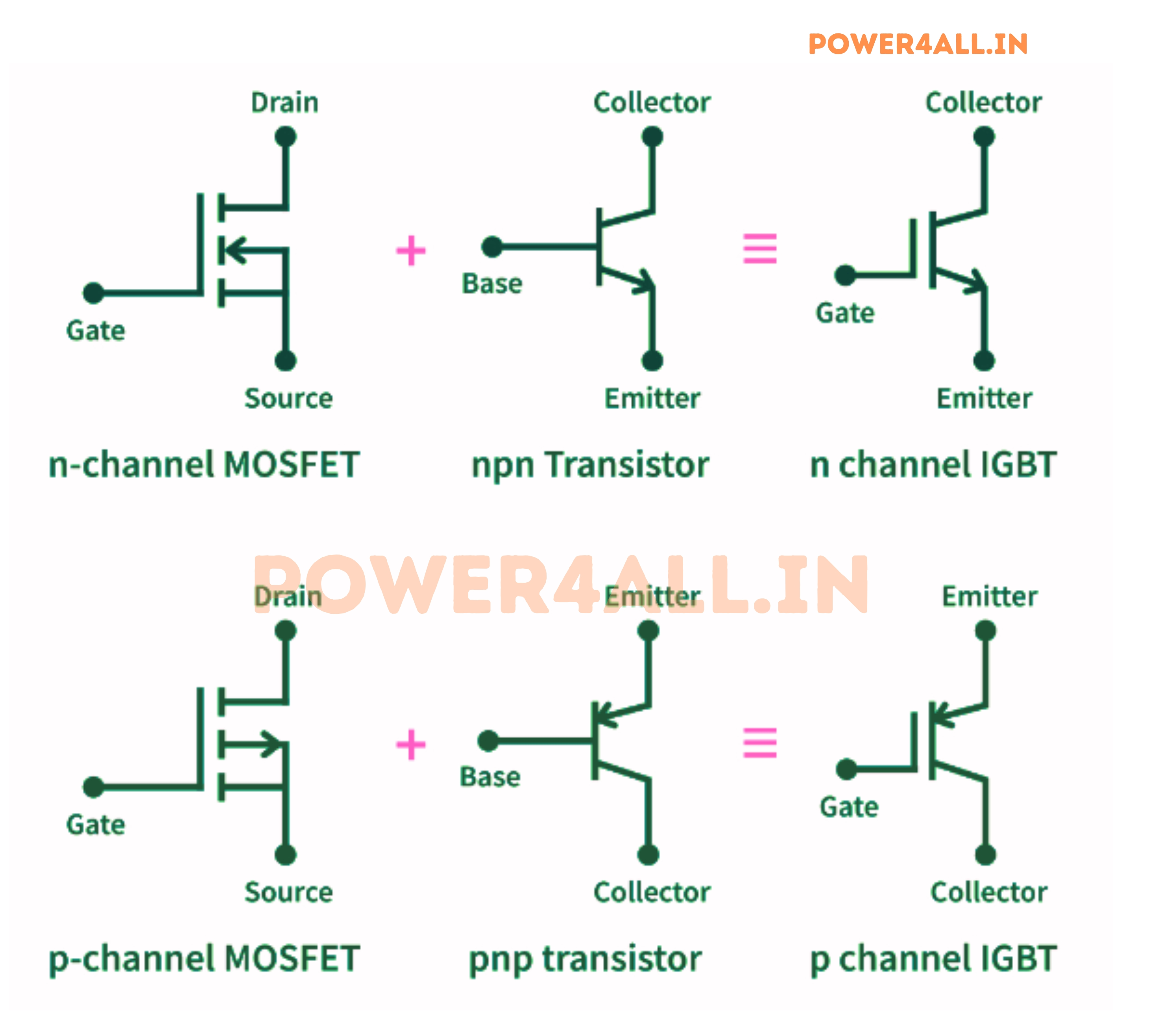
An IGBT (Insulated Gate Bipolar Transistor) is a three-terminal power semiconductor device that combines the best features of MOSFETs and BJTs. It offers the easy voltage drive of a MOSFET with the low conduction losses of a BJT, making it ideal for high-power, high-voltage switching applications in motor drives, inverters, and power supplies.
The Power Electronics Bridge
Think of an IGBT as a power electronic bridge that combines the voltage-controlled ease of a MOSFET input with the current-handling capability of a BJT output, creating the ideal device for high-power switching applications.
IGBT = MOSFET + BJT
- MOSFET input → High impedance gate control
- BJT output → Low voltage drop when conducting
- Voltage control → Easy to drive and control
- High current capability → Excellent for power applications
IGBT = MOSFET Gate + BJT Output
Best of both worlds for power switching applications
Why IGBTs Revolutionized Power Electronics
IGBTs filled a critical gap in power electronics by providing an efficient solution for medium to high power applications. Before IGBTs, engineers had to choose between easy-to-drive MOSFETs with high conduction losses or efficient BJTs with complex base drive requirements.
High Voltage Capability
IGBTs can handle voltages from 600V to 6500V, with some specialty devices reaching even higher voltages for HVDC applications.
High Current Handling
Modern IGBTs can switch currents from amperes to thousands of amperes, making them suitable for everything from motor drives to grid-tie inverters.
Voltage Controlled Operation
Like MOSFETs, IGBTs are voltage-controlled devices requiring minimal gate drive power, simplifying control circuit design.
Built-in Protection
Many modern IGBTs include built-in protection features like short circuit withstand capability and thermal shutdown.
IGBT Terminals and Symbol
Three Main Terminals
- Gate (G): Control terminal, voltage-controlled like MOSFET
- Collector (C): High voltage terminal, equivalent to drain in MOSFET
- Emitter (E): Current return path, equivalent to source in MOSFET
- Symbol: BJT symbol with insulated gate like MOSFET
- Current flow: Collector to Emitter when gate is positive
Operating Principle
- OFF state: No gate voltage, IGBT blocks current
- Turn-on: Positive gate voltage creates conduction
- ON state: Low voltage drop, high current capability
- Turn-off: Remove gate voltage, current stops
- Switching speed: Faster than BJT, slower than MOSFET
IGBTs in Modern Applications
- Electric vehicles: Traction inverters for motor control
- Industrial motors: Variable frequency drives (VFDs)
- Renewable energy: Solar and wind power inverters
- Railway systems: Traction control and regenerative braking
- Welding equipment: High-power inverter welders
- UPS systems: Uninterruptible power supplies
Historical Development
The IGBT was developed in the early 1980s by engineers at General Electric and later refined by multiple manufacturers. This innovation enabled the power electronics revolution we see today in electric vehicles, renewable energy, and efficient motor drives, making modern life possible through better energy management.
IGBT Fundamentals & Physics of Operation
Understanding IGBT operation requires exploring the unique combination of MOSFET input and BJT output structures. This hybrid design creates distinct operating characteristics that make IGBTs ideal for power electronics applications requiring both high voltage capability and efficient switching.
IGBT Internal Structure
Hybrid Device Architecture
An IGBT combines a MOSFET driving a BJT in a single silicon die. The MOSFET section provides voltage-controlled input, while the BJT section handles the main current conduction with low losses.
Physical Structure
- P+ substrate: Forms the collector region
- N- drift layer: Voltage blocking region
- P-body region: MOSFET channel area
- N+ source: Emitter connection point
- Gate oxide: Insulated gate control
IC = β × IB(MOSFET)
IGBT current amplification principle
Layer Functions
- Gate: Controls MOSFET channel formation
- N- drift: Supports high blocking voltage
- P+ substrate: Provides hole injection for BJT action
- Current flow: Holes from P+ and electrons from N+
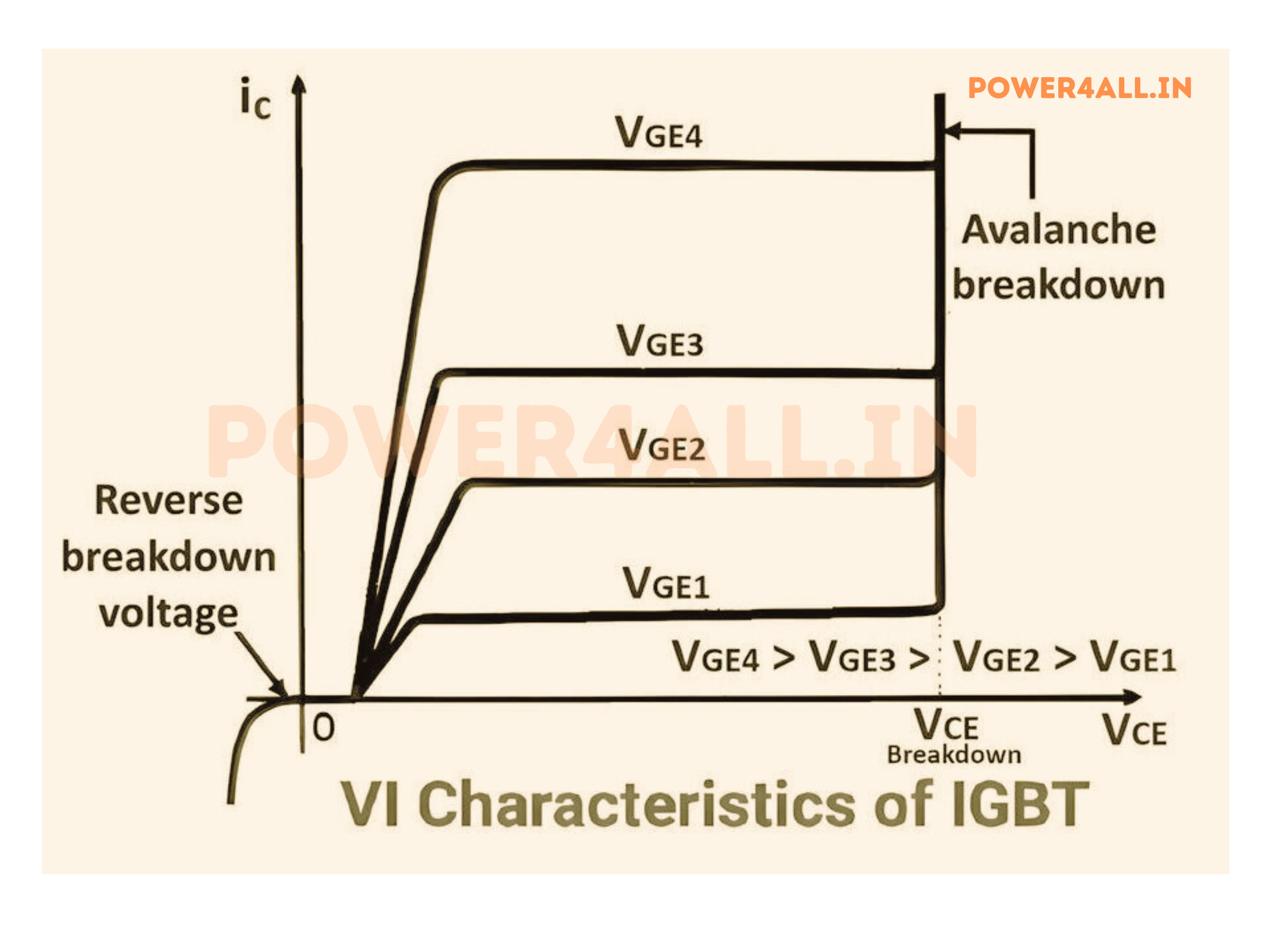
Operating Modes and Characteristics
IGBT Operating States and Transitions
Forward Blocking State
When the gate voltage is below threshold and collector voltage is positive, the IGBT blocks current flow.
| Parameter | Condition | Typical Value | Description |
|---|---|---|---|
| Gate Voltage | VGE < VTH | < 4-6V | Below threshold, no channel |
| Collector Current | IC ≈ ICES | < 1mA | Only leakage current |
| Collector Voltage | VCE = VDC | Up to VCES | Full applied voltage |
| Power Dissipation | P = VCE × ICES | < 10W | Very low losses |
Forward Conduction State
Turn-On Process
Positive gate voltage creates MOSFET channel, allowing current flow. This current becomes base current for internal BJT, which amplifies the total collector current.
Conduction Characteristics
Forward voltage drop typically 1.5-3V depending on current level and device rating. Much lower than power MOSFET at high currents.
Current Handling
High current density capability due to conductivity modulation in the drift region, allowing compact device design.
Switching Characteristics
Turn-On Behavior
IGBT turn-on sequence and timing
Turn-On Phases
- Delay time (td(on)): Gate charges to threshold voltage
- Current rise (tr): Collector current increases
- Voltage fall (tfv): Collector voltage decreases
- Tail current: Minority carrier buildup phase
Key Parameters
- Gate threshold: VTH = 4-6V typical
- Gate charge: QG = 50-500nC
- Turn-on time: ton = 0.1-2μs
- Turn-on energy: Eon ∝ VCE × IC × ton
ton = td(on) + tr + tfv
Total turn-on time components
Turn-Off Behavior
IGBT turn-off sequence and tail current
Turn-Off Phases
- Delay time (td(off)): Gate discharges to threshold
- Voltage rise (trv): Collector voltage increases
- Current fall (tf): Main current decreases
- Tail current: Minority carrier extraction
Tail Current Phenomenon
- Cause: Stored minority carriers in base region
- Duration: 1-10μs depending on device design
- Magnitude: 10-30% of rated current
- Impact: Increases turn-off losses
Loss Reduction Techniques
- Soft switching: Zero voltage/current switching
- Optimized gate drive: Controlled turn-off speed
- Clamp circuits: Limit overvoltage during turn-off
- Advanced IGBTs: Faster devices with reduced tail
IGBT Equivalent Circuit Model
Understanding IGBT Through Equivalent Circuit Analysis
Simplified Equivalent Circuit
The IGBT can be modeled as a MOSFET driving the base of a PNP BJT, with the BJT collector as the IGBT collector.
Circuit Components
- Input MOSFET: Voltage-controlled switch
- PNP BJT: Current amplification and conduction
- Base resistance: Limits MOSFET current
- Parasitic thyristor: Potential latch-up path
Current Flow Analysis
MOSFET Section
Gate voltage controls channel formation. Channel current becomes base current for the internal BJT section.
BJT Section
Base current from MOSFET is amplified by BJT current gain, providing high collector current capability.
Parasitic Thyristor
Inherent four-layer structure can form parasitic thyristor. Proper design prevents unwanted latch-up.
IC = β × ID(MOSFET)
Current amplification in IGBT equivalent circuit
Latch-Up Prevention
The parasitic thyristor in IGBT structure can cause latch-up under high current or high dI/dt conditions. Modern IGBTs include design features like lifetime control and optimized doping profiles to prevent this phenomenon.
IGBT Construction & Physical Structure
IGBT construction varies significantly based on voltage rating and application requirements. From planar gate structures for lower voltages to advanced trench designs for high-density applications, understanding the physical construction is essential for proper device selection and thermal management.
Silicon Die Construction
Layer-by-Layer Structure
IGBT fabrication requires precise control of multiple semiconductor layers, each optimized for specific electrical and thermal performance characteristics.
Layer Specifications
- P+ substrate: 200-400μm, 10¹⁹ atoms/cm³
- N- drift: 50-300μm, 10¹⁴ atoms/cm³
- P-body: 2-5μm, 10¹⁷ atoms/cm³
- N+ emitter: 0.5-2μm, 10²⁰ atoms/cm³
- Gate oxide: 50-100nm SiO₂
VCES ∝ (Thickness × Doping)^0.5
Voltage rating vs drift layer design
IGBT Structure Types
Planar Gate IGBT
Traditional horizontal gate structure
Design Features
- Gate structure: Horizontal polysilicon gate
- Channel: Formed at semiconductor-oxide interface
- Cell density: Lower than trench structures
- Voltage range: 600V to 6500V applications
Advantages
- Mature technology: Well-established manufacturing
- High voltage capability: Excellent for HV applications
- Ruggedness: Good short circuit withstand
- Cost effective: Lower manufacturing complexity
Limitations
- Higher on-voltage: Compared to trench designs
- Lower density: Larger chip area required
- Gate charge: Higher gate capacitance
Trench Gate IGBT
Advanced vertical gate technology
Design Features
- Gate structure: Vertical trench with gate oxide
- High density: More cells per unit area
- Better control: Improved channel control
- Voltage range: 600V to 1700V optimized
Advantages
- Lower VCE(sat): Reduced conduction losses
- Higher density: Smaller chip area
- Better switching: Lower gate charge
- Efficiency: Improved overall performance
Applications
- Motor drives: Variable frequency drives
- Solar inverters: High efficiency required
- UPS systems: Compact high-power designs
- Welding: High current switching
Advanced IGBT Technologies
Next-Generation IGBT Designs and Features
Reverse Conducting IGBT (RC-IGBT)
Integrates freewheeling diode functionality within the IGBT structure, reducing package complexity and improving performance.
Bidirectional Capability
Can conduct current in both directions when gate is off, eliminating need for external antiparallel diode.
Fast Recovery
Optimized for fast reverse recovery, reducing switching losses in hard-switching applications.
Compact Design
Single chip solution reduces package size and parasitic inductances compared to discrete solutions.
Field Stop IGBT
| Feature | Standard IGBT | Field Stop IGBT | Benefit |
|---|---|---|---|
| Wafer Thickness | Voltage dependent | Thinner wafer | Reduced losses |
| Voltage Blocking | Drift region only | Field stop + drift | Better control |
| Turn-off Losses | Higher | Lower | Improved efficiency |
| Tail Current | Longer | Shorter | Faster switching |
Light-Triggered IGBT
- Optical control: Light-activated gate triggering
- Isolation: Complete electrical isolation
- EMI immunity: Immune to electromagnetic interference
- Applications: High-voltage systems requiring isolation
Package Technologies
Discrete Packages
Individual IGBT devices
Common Package Types
- TO-247: 25A-100A, through-hole mounting
- TO-220: 10A-40A, cost-effective solution
- TO-264: 50A-150A, enhanced thermal performance
- SOT-227: 25A-50A, surface mount
Package Selection Criteria
- Current rating: Continuous and peak current
- Thermal resistance: RθJC specifications
- Isolation requirements: Voltage isolation needs
- Mounting method: Through-hole vs surface mount
Thermal Considerations
- TO-247: RθJC = 0.5-1.0°C/W
- TO-220: RθJC = 1.5-3.0°C/W
- Heat sink required: For most power applications
- Thermal interface: Use thermal compound
Power Modules
Integrated multi-device solutions
Module Configurations
- Half-bridge: Two IGBTs with antiparallel diodes
- Six-pack: Three-phase bridge configuration
- Seven-pack: Three-phase + brake chopper
- Intelligent modules: Integrated gate drivers
Module Advantages
- Matched devices: Optimized electrical characteristics
- Low inductance: Optimized internal layout
- Thermal management: Integrated cooling solutions
- Protection: Built-in monitoring and protection
Power Ranges
- Low power: 10A-50A modules
- Medium power: 100A-400A modules
- High power: 600A-3600A modules
- Custom: Application-specific designs
Thermal Design Importance
IGBT thermal design is critical for reliability and performance. Junction temperature directly affects switching losses, forward voltage drop, and device lifetime. Always ensure adequate thermal management through proper heat sink design and thermal interface materials.
Types of IGBTs and Classifications
IGBTs are classified based on their construction technology, voltage ratings, and specific application optimizations. Understanding these different types helps in selecting the optimal device for specific power electronics applications, from low-voltage motor drives to high-voltage HVDC systems.
Classification by Technology
Non-Punch-Through (NPT)
Standard IGBT technology
Design Characteristics
- Substrate: Lightly doped P+ collector
- Drift region: Uniform doping profile
- Voltage rating: Determined by drift layer thickness
- Turn-off: Slower due to wider base region
Advantages
- High voltage capability: 1200V to 6500V
- Ruggedness: Excellent short circuit withstand
- Reliability: Mature, proven technology
- Cost effective: Simpler manufacturing process
Applications
- High voltage drives: Industrial motor control
- Power transmission: HVDC converters
- Utility applications: Grid-tie inverters
- Railway traction: Locomotive drives
Punch-Through (PT)
Optimized for faster switching
Design Characteristics
- Buffer layer: N+ layer between drift and collector
- Thinner wafer: Reduced overall thickness
- Field shaping: Optimized electric field profile
- Faster switching: Reduced tail current
Advantages
- Lower losses: Reduced switching losses
- Faster switching: Shorter tail current
- Higher frequency: Better for high-frequency applications
- Efficiency: Improved overall efficiency
Applications
- Motor drives: Variable frequency drives
- UPS systems: High-frequency switching
- Solar inverters: Grid-tie applications
- Welding equipment: Inverter welders
Reverse Conducting (RC)
Integrated reverse diode functionality
Design Features
- Integrated diode: Built-in freewheeling diode
- Bidirectional: Can conduct in reverse when off
- Optimized recovery: Fast reverse recovery
- Single chip: Eliminates external diode
Benefits
- Reduced package count: No external diode needed
- Lower inductance: Optimized current paths
- Better thermal: Shared cooling for IGBT and diode
- Cost reduction: Simplified system design
Target Applications
- Matrix converters: Bidirectional switching
- Motor drives: Regenerative applications
- Grid converters: Bidirectional power flow
- Energy storage: Battery charge/discharge
Classification by Voltage Rating
| Voltage Class | Voltage Range | Typical Applications | Technology | Current Range |
|---|---|---|---|---|
| Low Voltage | 600V - 650V | Motor drives, UPS, welding | Trench, PT | 10A - 600A |
| Medium Voltage | 1200V - 1700V | Industrial drives, renewable | PT, Field Stop | 25A - 3600A |
| High Voltage | 3300V - 4500V | Traction, high power drives | NPT, Field Stop | 400A - 3000A |
| Ultra High Voltage | 6500V+ | HVDC, power transmission | NPT | 750A - 1500A |
IGBT Selection Guidelines
Selection Summary
Choose IGBTs based on voltage, current, switching speed, and thermal requirements. Consider application-specific needs such as short circuit withstand, switching frequency, and cost. Prototype and test to ensure optimal performance.
IGBT Operating Characteristics
IGBTs exhibit unique operating characteristics combining MOSFET and BJT behaviors. Understanding these characteristics is essential for designing efficient and reliable power electronics systems.
Static Characteristics
| Parameter | Symbol | Description | Typical Range |
|---|---|---|---|
| Collector-Emitter Voltage | V_CE | Voltage across collector and emitter terminals | 0 - V_CES(max) |
| Gate-Emitter Voltage | V_GE | Voltage applied to gate relative to emitter | 0 - 20V |
| Collector Current | I_C | Current flowing from collector to emitter | 0 - I_C(max) |
| Threshold Voltage | V_TH | Minimum gate-emitter voltage to turn on device | 4 - 6V |
| On-State Voltage Drop | V_CE(sat) | Voltage drop across device when fully on | 1.5 - 3V |
Switching Characteristics
Turn-On Time
Time taken for the IGBT to switch from off to on state.
- Delay time (td(on)): 0.1 - 1.5 µs
- Rise time (tr): 0.1 - 1.5 µs
- Total turn-on time (ton): td(on) + tr
Turn-Off Time
Time taken for the IGBT to switch from on to off state, including tail current.
- Delay time (td(off)): 0.1 - 1.5 µs
- Fall time (tf): 1 - 10 µs
- Tail current duration: 1 - 10 µs
- Total turn-off time (toff): td(off) + tf + tail current
Safe Operating Area (SOA)
IGBTs must be operated within their SOA to prevent damage. This includes limits on voltage, current, power dissipation, and temperature.
SOA Considerations
- Maximum collector current and voltage
- Short circuit withstand capability
- Thermal limits and cooling requirements
- Switching frequency and losses
Operating Outside SOA
Exceeding SOA limits can cause device failure due to thermal runaway, latch-up, or electrical overstress. Always design with adequate safety margins.
IGBT vs MOSFET vs BJT Comparison
Comparing IGBTs with MOSFETs and BJTs helps in selecting the right device for specific power electronics applications based on voltage, current, switching speed, and efficiency requirements.
Device Comparison Table
| Parameter | IGBT | MOSFET | BJT |
|---|---|---|---|
| Control Type | Voltage controlled | Voltage controlled | Current controlled |
| Input Impedance | High | Very high | Medium |
| Switching Speed | Medium (µs range) | Fast (ns range) | Medium (ns-µs range) |
| Conduction Losses | Low (due to BJT conduction) | Higher (due to RDS(on)) | Medium |
| Voltage Rating | 600V to 6500V+ | 20V to 1700V | Low to medium |
| Current Rating | High (up to kA) | Medium to high | Medium |
| Applications | High power inverters, motor drives, HVDC | Switching power supplies, low voltage drives | Amplifiers, low power switching |
Application Recommendations
- Use IGBTs for high voltage, high current, and medium frequency applications.
- Use MOSFETs for low voltage, high frequency, and low power applications.
- Use BJTs for linear amplification and low power switching.
Design Considerations
Consider switching losses, gate drive complexity, and thermal management when selecting devices. Hybrid solutions may be optimal for specific applications.
IGBT Power Electronics Applications
IGBTs are widely used in power electronics for efficient control of high voltage and high current systems. Their applications span industrial motor drives, renewable energy inverters, electric vehicles, and more.
Industrial Motor Drives
Variable Frequency Drives (VFDs)
Precise speed and torque control
Key Features
- High efficiency and reliability
- Wide power range from small to large motors
- Regenerative braking capability
- Advanced control algorithms
VFD Example
- Power rating: 0.5kW to 10MW
- Switching frequency: 1kHz to 20kHz
- IGBTs used: 600V to 1700V devices
- Applications: Pumps, fans, conveyors, compressors
Traction Drives
Electric and hybrid vehicle propulsion
Key Features
- High power density and efficiency
- Robustness for harsh environments
- Fast switching and control
- Integrated protection features
Traction Drive Example
- Power rating: 50kW to 1MW+
- IGBTs used: 1200V to 3300V devices
- Applications: Trains, trams, electric buses
Renewable Energy Systems
Solar Inverters
Converting DC from solar panels to AC grid power
Key Features
- High efficiency and reliability
- Grid synchronization and power factor control
- Wide voltage and power range
- Advanced MPPT algorithms
Solar Inverter Example
- Power rating: 1kW to 1MW+
- IGBTs used: 600V to 1700V devices
- Applications: Residential, commercial, utility-scale
Wind Turbine Converters
Power conversion and grid integration
Key Features
- High voltage and current handling
- Robustness for harsh environments
- Fast switching and control
- Integrated protection features
Wind Converter Example
- Power rating: 100kW to 10MW
- IGBTs used: 1200V to 4500V devices
- Applications: Onshore and offshore wind turbines
Other Applications
- Uninterruptible Power Supplies (UPS)
- Welding Equipment
- Induction Heating
- Power Factor Correction (PFC) Circuits
- Electric Traction and Transportation
Market Trends
The IGBT market is growing rapidly due to increasing demand in electric vehicles, renewable energy, and industrial automation. Advances in device technology continue to improve efficiency and reduce costs.
IGBT Gate Drive & Control
Proper gate drive and control circuits are essential for reliable and efficient IGBT operation. This section covers gate drive requirements, protection, and common control techniques.
Gate Drive Requirements
- Gate voltage typically 15V for full turn-on
- Gate current sufficient to charge/discharge gate capacitance quickly
- Low impedance drive to minimize switching losses
- Protection against overvoltage and negative voltage spikes
Gate Drive Circuits
Isolated Gate Drivers
Provide galvanic isolation between control and power circuits, improving safety and noise immunity.
- Optocoupler or transformer-based isolation
- Integrated protection features
- High peak current capability
- Common devices: IR2110, UCC37322
Non-Isolated Gate Drivers
Simple, cost-effective drivers for low voltage or single-ended applications.
- Direct microcontroller or logic gate drive
- Gate resistors for switching control
- Protection diodes and snubbers
- Common devices: TC4420, MIC4452
Gate Protection Techniques
- Gate resistors to limit inrush current and reduce EMI
- Zener diodes or TVS diodes to clamp gate voltage
- Negative voltage clamps to ensure complete turn-off
- Proper PCB layout to minimize parasitic inductance
Gate Drive Best Practices
Use appropriate gate drive voltage and current, include protection components, and ensure clean, fast switching to minimize losses and prevent device damage.
IGBT Selection & Design Guide
Selecting the right IGBT involves balancing voltage, current, switching speed, thermal management, and cost. This guide provides key parameters and design considerations for optimal device choice.
Key Parameters to Consider
- Voltage rating (V_CES)
- Continuous collector current (I_C)
- Switching times and losses
- Thermal resistance and cooling requirements
- Safe operating area (SOA)
- Package type and mounting
Design Considerations
- Derate voltage and current ratings for safety margin
- Ensure adequate gate drive voltage and current
- Design for efficient thermal management
- Consider switching frequency and losses
- Use protection circuits for overcurrent and overvoltage
Selection Example
For a 1200V, 100A motor drive application, choose an IGBT with at least 1500V voltage rating, 120A current rating, low V_CE(sat), and suitable package for heat dissipation.
IGBT Testing & Troubleshooting
Effective testing and troubleshooting are essential for reliable IGBT operation. This section covers basic tests, advanced diagnostics, and common failure modes.
Basic Testing Methods
- Multimeter diode test for body diode and gate insulation
- Gate-emitter voltage measurement
- Collector-emitter resistance check
- Functional switching test with load
Advanced Testing Techniques
- Curve tracer for I-V characteristics
- Oscilloscope for switching waveforms
- Thermal imaging for hot spots
- Parametric testing for threshold voltage and gain
Common Failure Modes
- Gate oxide breakdown due to ESD or overvoltage
- Thermal runaway from inadequate cooling
- Latch-up due to parasitic thyristor action
- Short circuit and overcurrent damage
Testing Safety
Always discharge gate capacitance before testing, use ESD protection, and ensure power is off before making measurements.
IGBT Safety Considerations
Safety is paramount when working with IGBTs due to high voltages, currents, and thermal stresses. Proper handling, protection, and thermal management are essential to prevent damage and ensure operator safety.
Electrical Safety
- Observe maximum gate and collector voltage ratings
- Use proper isolation and grounding techniques
- Implement overcurrent and overvoltage protection
- Discharge capacitors before servicing
Thermal Safety
- Use adequate heat sinking and cooling systems
- Monitor junction and case temperatures
- Provide warning labels for hot surfaces
- Use thermal protection circuits
ESD Protection
- Use ESD-safe workstations and tools
- Wear grounded wrist straps and use antistatic mats
- Store and transport devices in antistatic packaging
High Voltage Warning
IGBT circuits often operate at lethal voltages. Always follow electrical safety codes and use appropriate personal protective equipment (PPE).
Frequently Asked Questions about IGBTs
Answers to common questions about IGBT operation, selection, and troubleshooting to help engineers and students understand these devices better.
Basic Questions
What is the main advantage of IGBTs over MOSFETs?
IGBTs combine the high input impedance of MOSFETs with the low conduction losses of BJTs, making them more efficient for high voltage and high current applications.
Why are IGBTs slower than MOSFETs?
IGBTs have slower switching speeds due to the minority carrier injection in the BJT portion, which causes tail current during turn-off, increasing switching losses.
What gate voltage is required to turn on an IGBT?
Typically, a gate-emitter voltage of 15V is used to fully turn on an IGBT. Gate drive circuits must provide sufficient current to charge the gate capacitance quickly.
What are common failure modes of IGBTs?
- Gate oxide breakdown due to ESD or overvoltage
- Thermal runaway from inadequate cooling
- Latch-up due to parasitic thyristor action
- Short circuit and overcurrent damage
Mastering IGBT Technology: Your Path to Efficient Power Electronics
IGBTs are essential components in modern power electronics, enabling efficient control of high voltage and high current systems. Mastering their operation, characteristics, and applications opens doors to advanced power system design and innovation.
Key Takeaways
Hybrid Device Advantages
IGBTs combine MOSFET input with BJT output for efficient high power switching.
Wide Application Range
Used in motor drives, inverters, renewable energy, and industrial power systems.
Design Considerations
Proper gate drive, thermal management, and protection circuits are essential for reliable operation.
Future Trends
Advances in materials and device structures continue to improve IGBT performance and efficiency.
Thank you for exploring the world of Insulated Gate Bipolar Transistors!
Continue your power electronics journey with our other comprehensive guides and resources.