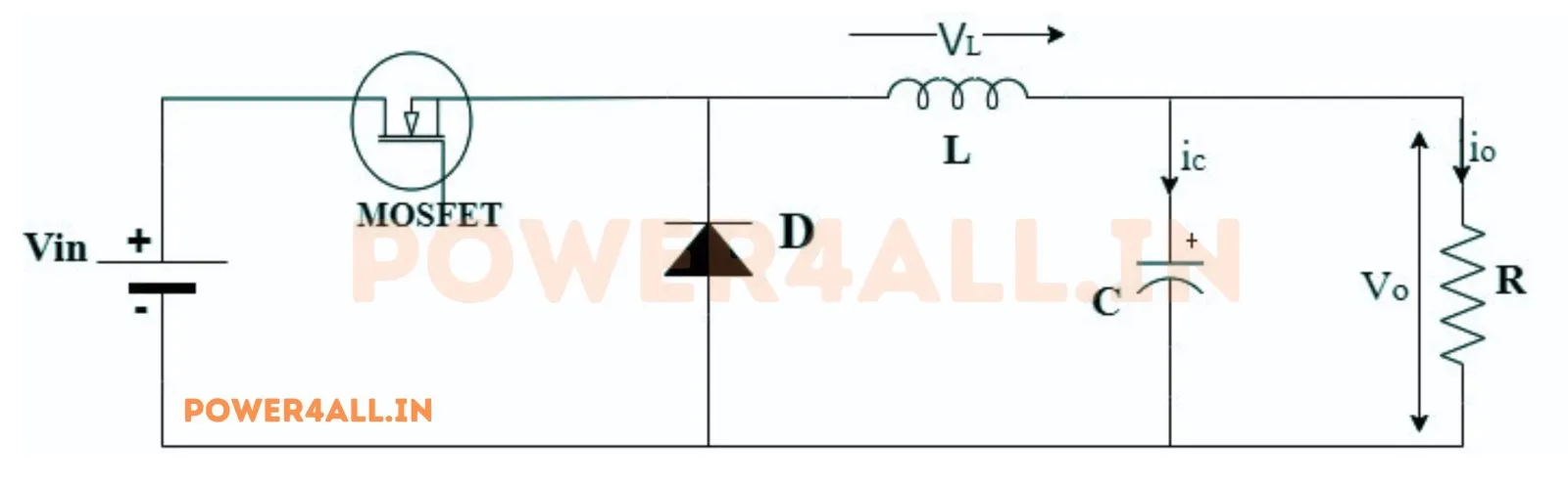
What is a buck (step-down) converter?
A buck converter is a switched-mode DC-DC converter that produces an output voltage lower than its input. A transistor (usually a power MOSFET) switches the input on and off at a high frequency; a freewheeling diode (or a second, synchronous MOSFET) provides a path for the inductor current when the switch is off; and an L-C filter smooths the chopped switch-node voltage into a clean DC output. Because the energy is handled by (almost) lossless reactive components rather than being dropped across a resistor, a buck converter is far more efficient than a linear regulator — typically 90–98%.
How it works — the two switching states
Over each switching period T = 1/fsw the converter alternates between two states set by the duty cycle D (the fraction of the period the switch is ON):
- Switch ON (0 → D·T): the MOSFET connects the inductor to Vin; the inductor current ramps up as
diL/dt = (Vin − Vo)/L, storing energy and delivering current to the load. - Switch OFF (D·T → T): the MOSFET is off, the diode conducts, and the inductor current ramps down as
diL/dt = −Vo/L, releasing its stored energy into the load.
Key equations
This simulator does not plug numbers into these formulas — it numerically integrates the real switching circuit (with your device parasitics) to steady state, then measures Vo, the ripple and the losses from the resulting waveforms and compares them to the equations above in the accuracy panel.
Continuous vs discontinuous conduction (CCM / DCM)
In CCM the inductor current never falls to zero and Vo = D·Vin holds. At light load or with a small inductor the current hits zero each cycle — DCM — the diode stops conducting, and the output voltage rises above D·Vin. The boundary is the critical inductance Lc = (1 − D)·R/(2·fsw). Try the Light load → DCM preset and watch the inductor current touch zero.
Efficiency & losses
Real converters lose power in the MOSFET (Rds(on) conduction and switching losses), the diode (forward-voltage drop Vf), the inductor (winding resistance DCR and core loss) and the capacitor (ESR). This simulator computes the conduction losses exactly from the integrated currents and shows the split in the loss-breakdown chart, so you can see which component to improve first. Add the device parasitics and watch the efficiency fall from 100%.
Buck vs boost vs buck-boost
| Converter | Output vs input | Ideal Vo |
|---|---|---|
| Buck | Steps down (Vo < Vin) | D·Vin |
| Boost | Steps up (Vo > Vin) | Vin/(1 − D) |
| Buck-Boost | Up or down, inverted | −D·Vin/(1 − D) |
Applications
Point-of-load regulators on almost every PCB (5 V → 3.3 V / 1.8 V / 1.2 V), laptop and phone power rails, LED drivers, battery chargers, motor-drive supplies, solar MPPT stages and automotive 12 V → 5 V converters. The buck is the most common DC-DC topology in electronics.
Frequently asked questions
What is the output voltage of a buck converter?
In CCM the ideal output is Vo = D·Vin, always lower than the input. Real device drops make it slightly lower; the simulator shows both.
What is the inductor ripple current?
ΔiL = (Vin − Vo)·D/(L·fsw) = Vo·(1 − D)/(L·fsw). A bigger inductor or higher switching frequency reduces it.
What causes discontinuous conduction (DCM)?
Light load or a small inductor lets the inductor current reach zero each cycle. Below the critical inductance Lc = (1−D)·R/(2·fsw) the converter enters DCM and the output rises above D·Vin.
How do I reduce output-voltage ripple?
Increase C or fsw (ΔVo = ΔiL/(8·C·fsw)), reduce ΔiL with a larger L, and use a low-ESR capacitor — in real designs the ESR term ΔiL·ESR usually dominates.
Why is a buck converter efficient?
It stores and transfers energy with a lossless inductor and capacitor instead of dropping the excess voltage as heat like a linear regulator. Losses come only from device resistances and the diode drop — shown in the loss-breakdown chart.