Half-Bridge Converter
The split-rail isolated buck — a capacitor divider makes a half-voltage rail, and two series switches drive the transformer with only ±Vin/2. Each switch is stressed to just Vin, half of a push-pull, which makes it the natural choice for off-line, mid-power supplies.
- Introduction — a push-pull at half the voltage
- What is a Half-Bridge Converter?
- Block Diagram
- Circuit Diagram & Construction
- Principle of Operation
- Modes of Operation
- Waveforms Explained in Detail
- Capacitor Selection & Automatic Flux Balancing
- Key Formulas
- Voltage Gain & Turns Ratio
- Worked Example
- Advantages & Disadvantages
- Applications
- Frequently Asked Questions – FAQs
- Related Topics
Introduction — a push-pull at half the voltage
The push-pull converter is a great mid-power workhorse, but it has one stubborn drawback: each switch has to block twice the input voltage. When you run from a rectified AC line — a bus of 300–400 V — that means 800 V transistors, which are slow and expensive. The half-bridge converter solves this with a neat trick. Instead of a centre-tapped primary driven from the full rail, it splits the input across two series capacitors to make a half-voltage mid-rail, and hangs a single-primary transformer between that mid-rail and a pair of series switches.
The result: the primary swings only ±Vin/2, and each switch never sees more than Vin — half a push-pull’s stress. That single change is what makes the half-bridge the default topology for off-line supplies in the 100 W–500 W range. It keeps the push-pull’s good points — a symmetric AC drive that uses the core in both directions, an output fed twice per cycle, a small filter — and adds a bonus: a small series coupling capacitor that blocks DC and keeps the transformer flux balanced all by itself.
This page builds the half-bridge from that idea: the split-rail capacitor divider, the two series switches, the DC-blocking capacitor, what happens in each switching state, the waveforms you would see on a scope, how to size the capacitors (the question that trips most first-time designers), the formulas that set the output, and a full worked example with real numbers.
What is a Half-Bridge Converter?
A half-bridge converter is an isolated switch-mode DC-DC converter that behaves like a buck converter fed by two alternating switches through a transformer, where the primary is driven at only half the input voltage. It is built from these parts:
- A capacitor divider, C1 and C2. Two equal capacitors in series across Vin. Their junction (node M) sits at Vin/2 — the half-voltage mid-rail that gives the topology its name.
- Two switches (MOSFETs), Q1 and Q2, in series across Vin. Their junction (node A) is the switching node. Q1 is the high-side switch, Q2 the low-side; they conduct alternately, 180° apart.
- A single-primary transformer connected between node A and node M, so it is driven with a ±Vin/2 square wave. Because it is driven both ways it needs no reset winding.
- A small DC-blocking (coupling) capacitor, Cb, in series with the primary. It passes the AC drive but blocks any DC, which automatically stops the core from saturating.
- Two rectifier diodes, D1 and D2, forming a full-wave rectifier on a centre-tapped secondary, feeding an output L-C filter exactly as in a buck.
The heart of it is the half-voltage drive. When Q1 turns on, node A rises to Vin, so the primary sees Vin − Vin/2 = +Vin/2. When Q2 turns on, node A falls to 0, so the primary sees 0 − Vin/2 = −Vin/2. The primary is therefore driven back and forth with half the rail, and — crucially — whichever switch is off only ever sees the full Vin, never more.
Block Diagram
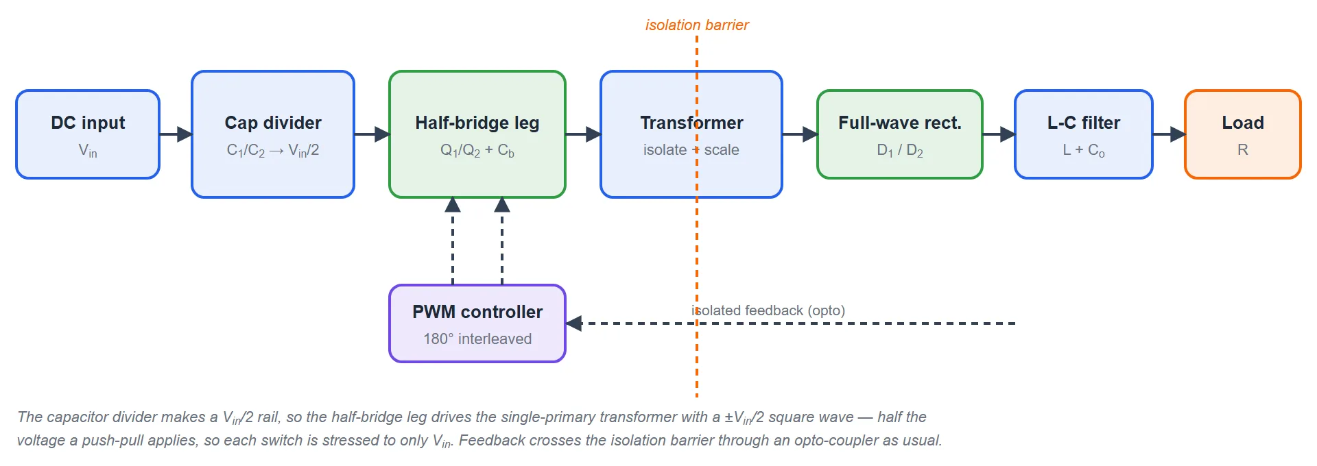
Read it left to right as a power path: the DC input is split by the capacitor divider into a half-voltage rail, chopped by the two series switches, driven through the transformer (via the DC-blocking capacitor), full-wave rectified, smoothed by the L-C filter, and delivered to the load. Two things mark it as a half-bridge. First, the divider that produces the Vin/2 mid-rail. Second, the transformer is driven with a ±Vin/2 square wave, so each switch blocks only Vin. As always, feedback crosses the isolation barrier through an opto-coupler.
Circuit Diagram & Construction
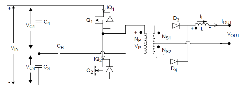
Following the drawing across (this is the circuit described in the source design question), the power path is easy to trace:
| Capacitor divider C1, C2 | Two equal bulk capacitors in series across Vin. Their junction, node M, sits at Vin/2 and is one end of the transformer primary. They also carry the primary’s AC current each half-cycle, so they must be large and low-impedance (see the capacitor-selection section below). |
|---|---|
| Switches Q1, Q2 | Two switches in series across Vin; their junction is node A. Q1 (high-side) needs a floating gate drive; Q2 (low-side) is ground-referenced. They conduct alternately (180° apart) and must never overlap. Each blocks only Vin when off. |
| DC-blocking capacitor Cb | A small film capacitor in series with the primary. It couples the AC drive but passes no DC, so it prevents any net volt-second imbalance from magnetising the core — automatic flux balancing. |
| Transformer (single primary Np) | Driven between node A and node M, so it sees ±Vin/2. Because the drive is symmetric AC, the core swings both ways and needs no reset winding or air gap. n = Ns/Np sets the coarse voltage scaling. |
| Rectifier diodes D1, D2 | Full-wave rectifier on the centre-tapped secondary. D1 conducts with Q1, D2 with Q2, and both conduct together (sharing the inductor current) during the dead time. Each blocks n·Vin. |
| Output filter L, Co | A buck-type L-C filter. The output is fed twice per period, so the inductor current ripples at twice the switching frequency and the filter can be small. |
Principle of Operation
The two switches are driven by the same PWM controller but 180° out of phase, each on for a fraction D of the full period (D < 0.5). Over one period there are four intervals: Q1 on, dead time, Q2 on, dead time. The capacitor divider, the transformer and the output inductor split the work:
- When Q1 is on, node A is pulled up to Vin, so the primary sees +Vin/2. A scaled voltage n·Vin/2 appears on the secondary, D1 conducts, and energy passes straight through to the L-C filter. The inductor current ramps up.
- When Q2 is on, node A is pulled down to 0, so the primary sees −Vin/2 — the opposite polarity. The same n·Vin/2 reaches the filter, this time through D2. The inductor charges again.
- In the dead time (both off), the transformer is quiet, but the output inductor keeps its current flowing — and with no switch driving, both diodes conduct together, each carrying half the inductor current back to the load. This is the freewheel.
So the load sees an energy pulse twice per switching period, and the transformer sees a symmetric AC square wave at half the rail. The output voltage is fixed, as in a buck, by volt-second balance on the output inductor. The series capacitor Cb guarantees the two half-cycles carry equal volt-seconds, so the core’s flux stays centred without any reset winding.
Modes of Operation
A half-bridge has two driven states — one per switch — separated by a short dead time in which both switches are off and the output inductor freewheels. Trace each state on the power circuit of Figure 2 above; the current path is described in words below.
Mode 1 — Q1 ON (high-side drives)
- Q1 connects node A to Vin. Current flows from the + rail through Q1 to node A, through the DC-blocking capacitor Cb and the primary to node M, and back through the lower capacitor C2. The primary sees +Vin/2 and the core magnetises in the “positive” direction.
- On the secondary, n·Vin/2 forward-biases D1. The inductor sees (n·Vin/2 − Vo) and its current ramps up, delivering power to the load.
- Q2 and D2 are off. The idle switch Q2 holds off exactly Vin — no more, because node A is clamped at Vin.
Mode 2 — Q2 ON (low-side drives)
- Half a period later Q2 connects node A to ground. Current now flows from node M through the primary and Cb to node A and down through Q2, with the upper capacitor C1 supplying it. The primary sees −Vin/2 — the opposite polarity — so the core magnetises the other way, which resets it.
- The secondary now produces n·Vin/2 in the opposite sense, forward-biasing D2, so the inductor charges just as it did in Mode 1. From the output’s point of view Modes 1 and 2 are identical.
- Q1 and D1 are off, and Q1 now holds off Vin.
Dead time — both off (freewheel)
- Between the two driven states, both switches are off for a short guard interval. The transformer delivers no power, but the output inductor keeps its current flowing.
- With neither half driven, the inductor current divides equally between the two secondary halves, so both rectifier diodes D1 and D2 conduct together, each carrying half the inductor current. The secondary is effectively shorted, so the inductor sees −Vo and its current ramps gently down until the next switch turns on.
- This freewheel keeps the output current continuous — the same job a buck converter’s freewheel diode does — and the switching node A settles to about Vin/2.
Waveforms Explained in Detail
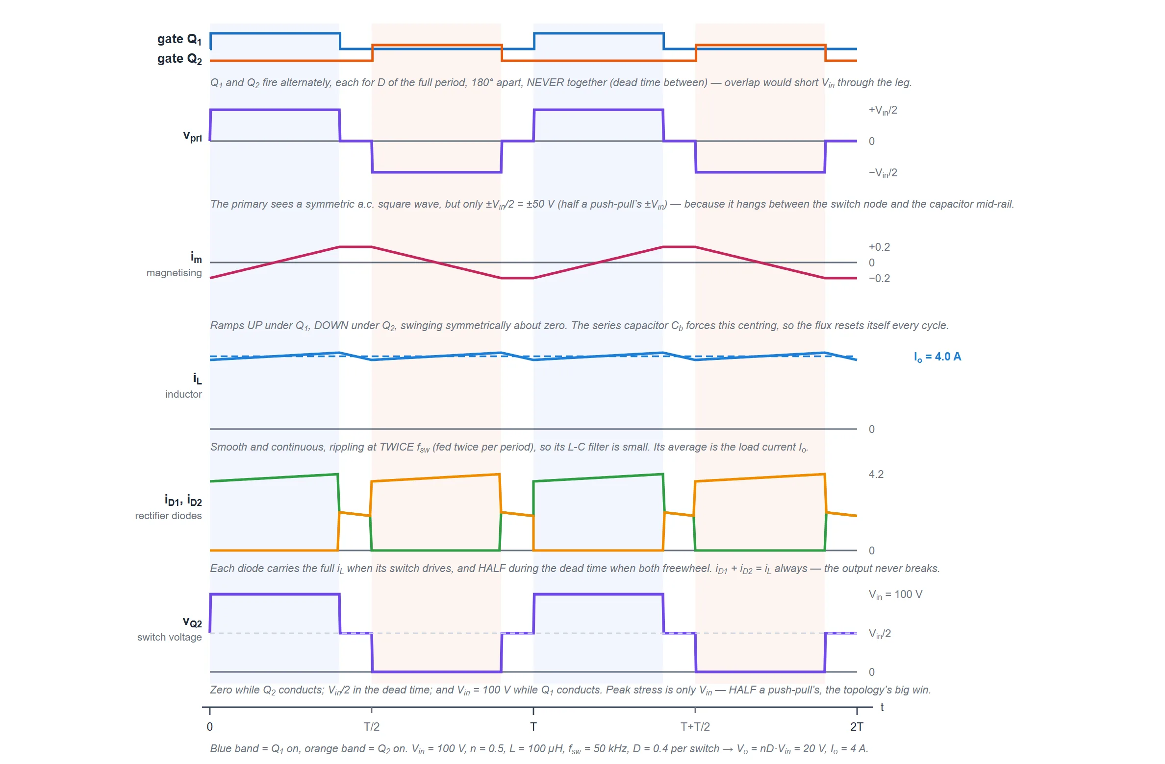
Read the traces together and the whole converter is visible in one picture:
- Gates Q1, Q2. Two pulses, each on for D of the full period, 180° apart, with a dead gap between them. They never overlap — the gap is the shoot-through guard.
- Primary voltage vpri. A symmetric AC square wave, but only ±Vin/2 (±50 V here): +Vin/2 under Q1, −Vin/2 under Q2, zero in the dead time. Half a push-pull’s primary swing — the whole point of the topology.
- Magnetising current im. Ramps up under Q1 and down under Q2, swinging symmetrically about zero. The series capacitor Cb forces this centring, so the flux returns to where it started every period.
- Inductor current iL. A smooth triangle that never reaches zero, rippling at twice the switching frequency because the filter is topped up twice per period. Its average is the load current.
- Diode currents iD1, iD2. Each carries the full inductor current while its switch drives, and half during the dead-time freewheel. At every instant iD1 + iD2 = iL, so the output current never breaks.
- Switch voltage vQ2. Zero while Q2 conducts, Vin/2 in the dead time, and Vin = 100 V while Q1 conducts. The peak stress is only Vin — exactly half a push-pull’s 2·Vin, and the reason the half-bridge is preferred off-line.
Capacitor Selection & Automatic Flux Balancing
The half-bridge lives and dies by its capacitors, and choosing them is the question most first-time designers ask. There are two very different capacitors in the circuit, and they do very different jobs.
1. The divider capacitors C1, C2 (the bulk / bridge caps)
These two carry the transformer’s primary current on alternate half-cycles while holding the mid-rail at Vin/2. If they are too small, the mid-rail sags during each on-time and the output droops. They are sized from the allowed ripple voltage: the charge drawn during one on-time, divided by the capacitance, must stay small.
ΔVC ≈ (Ipri · D · T) / C → C ≥ (Ipri · D · T) / ΔVC,allowedIn practice this lands on large bulk capacitors. A common rule of thumb is roughly 1 µF per watt of output power, so a ~400 W design typically uses two capacitors of about 470 µF–680 µF in series. They must also be rated for the full ripple current they carry, so low-ESR electrolytics (often paralleled with a film cap) are usual. On an off-line supply these are frequently the same bulk capacitors that filter the rectified line, split into two.
2. The DC-blocking capacitor Cb (the coupling cap)
This small capacitor sits in series with the primary. It couples the AC drive through untouched but blocks any DC, and that is what gives the half-bridge its quiet superpower: automatic flux balancing. If the two half-cycles ever carry slightly unequal volt-seconds — because one switch is a touch slower, or has a lower on-state drop — Cb simply charges to a small DC offset that cancels the difference, and the core cannot “walk” into saturation the way an uncorrected push-pull can.
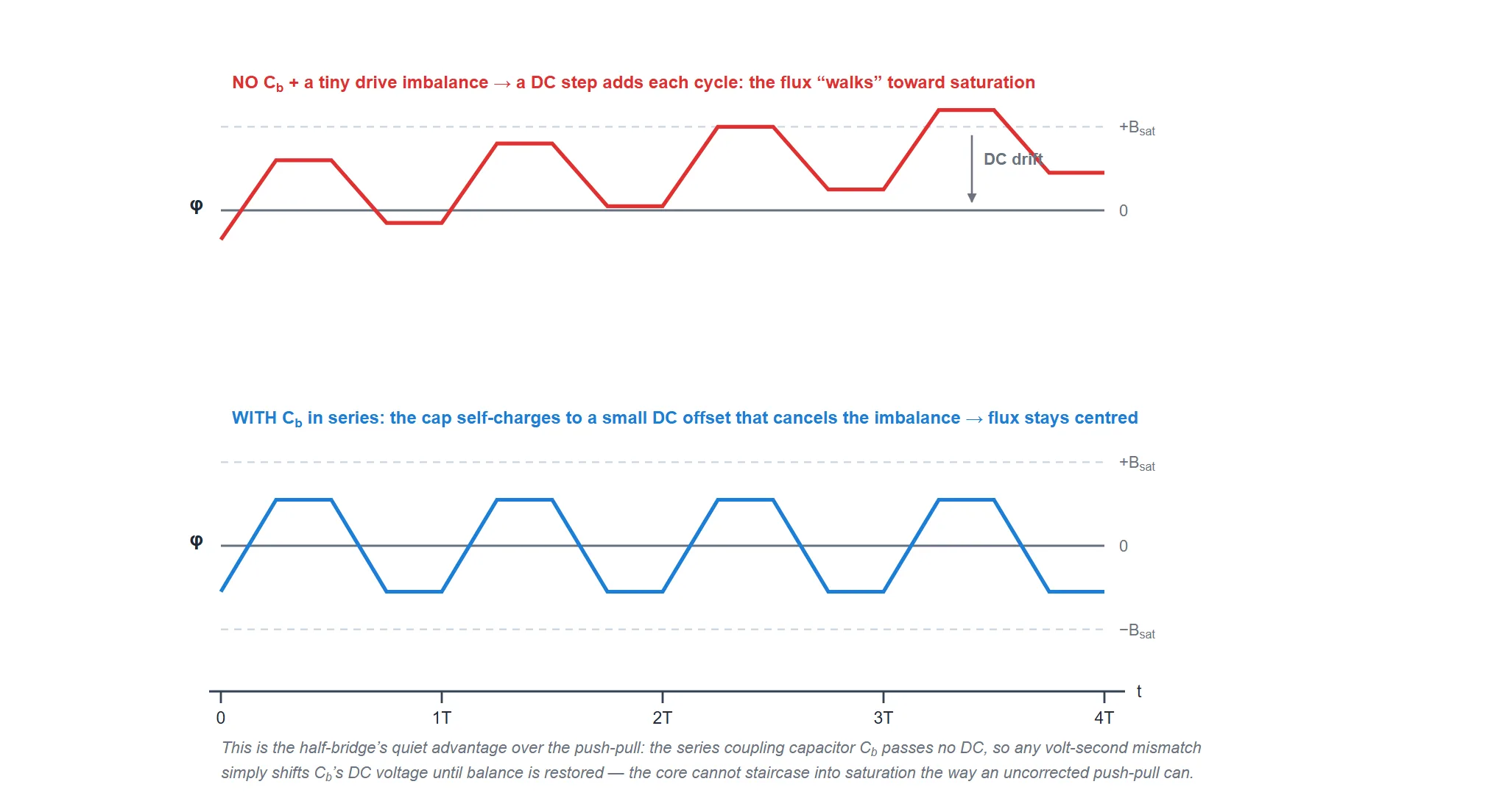
Cb is a small film capacitor, typically 0.47 µF–1 µF, rated comfortably above half the peak bus voltage. For a universal-input off-line supply whose AC input ranges 185–265 V (a rectified DC bus of roughly 370 V), a 1 µF / 250 V film cap is a typical choice. It should be big enough to couple the drive without dropping much AC voltage across itself, but small enough to respond quickly to any imbalance.
Key Formulas
All of these come from volt-second balance on the output inductor, with n = Ns/Np and D the duty of each switch (D ≤ 0.5).
Output voltage (CCM). The filter is fed n·Vin/2 for a total of 2D of the period (two pulses) and 0 for the rest; the inductor’s average voltage is zero:
(n·Vin/2 − Vo)·2D·T = Vo·(1 − 2D)·T → Vo = n · D · VinA straight line in D, like a buck, and exactly HALF a push-pull’s Vo = 2nD·Vin at the same turns ratio — because the primary swings Vin/2, not Vin.
Duty ratio for a target output. Rearranging:
D = Vo / (n · Vin) (must stay < 0.5)Inductor-current ripple and average. Standard buck filter, ripple repeating every half period:
ΔiL = (n·Vin/2 − Vo)·D·T / L | IL,avg = IoDevice stress. The idle switch sees only the full rail; the off diode sees the reflected opposite half:
Switch: VQ,off = Vin | Diode: VD,rev = n · VinCurrents. Each switch carries the reflected inductor current during its on-time; the divider caps smooth the DC drawn from the source:
IQ,avg ≈ D · n · Io | Iin,avg = n · D · Io = Po / VinCapacitor sizing. Divider ripple and the coupling-cap rating:
C1,2 ≥ (Ipri·D·T) / ΔVC (≈ 1 µF/W) | Cb ≈ 0.47–1 µF, Vrating > Vin/2(Switch and diode drops, winding resistance and losses are neglected here; a real half-bridge is typically 88–93 % efficient.)
Voltage Gain & Turns Ratio
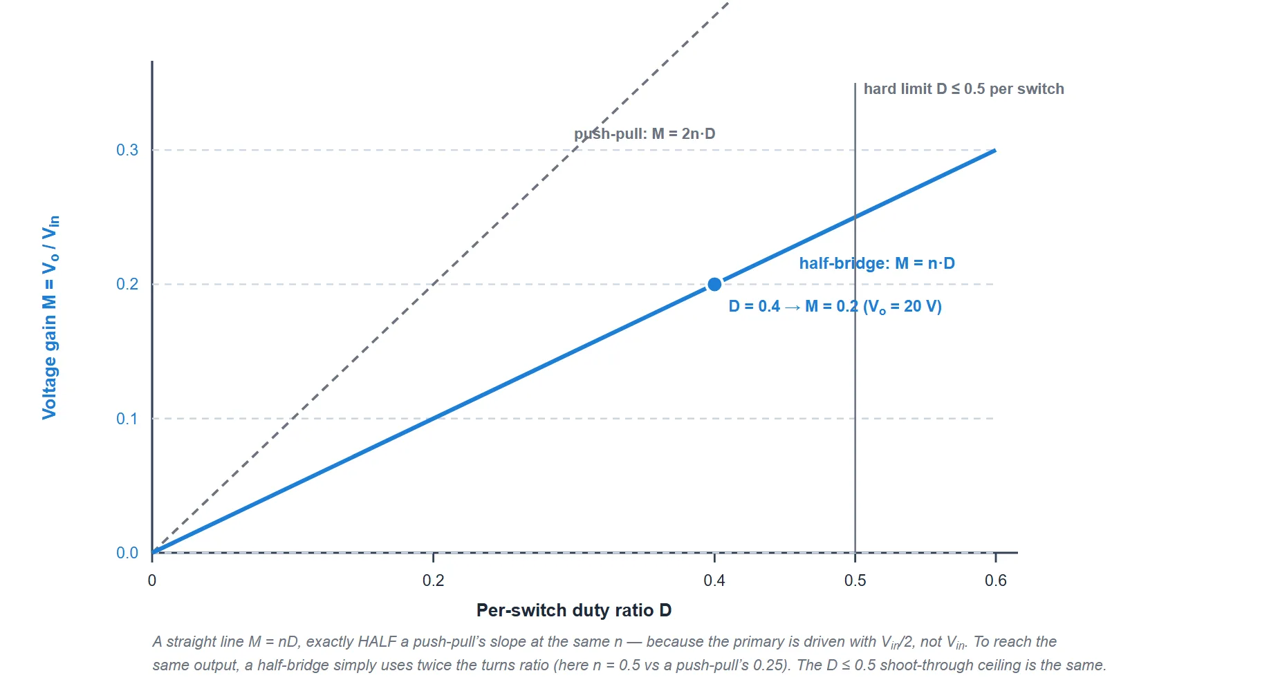
The half-bridge’s gain is a straight line, M = n·D — easy to control, and exactly half the gain of a push-pull converter at the same turns ratio and duty, because the primary is driven with Vin/2 instead of Vin. To reach the same output, the half-bridge simply uses twice the turns ratio. Like the forward and push-pull it is fundamentally a step-down. Key points:
- The turns ratio sets the operating point. An off-line supply dropping a ~400 V bus to a low output picks n so the duty lands comfortably below the 0.5 limit.
- The duty is hard-capped at 0.5 per switch. Above it the switches would overlap and short the leg, so the maximum output is n·Vin/2. Real designs leave margin for dead time, so the practical ceiling is a little below 0.5.
- Continuous inductor current keeps it linear. As in any buck-derived converter, very light load can push the inductor into discontinuous conduction, where the output rises above n·D·Vin and depends on load. The inductor is sized to stay continuous over the load range.
Worked Example
One consistent design, used by every figure above. Follow the numbers and the formulas check out.
| Given | Vin = 100 V (dc bus), Ns:Np = 1:2 (n = 0.5), D = 0.4 per switch, f = 50 kHz (T = 20 µs), L = 100 µH, Lm = 1 mH |
|---|---|
| Primary swing ±Vin/2 | ±50 V (half a push-pull’s ±Vin) |
| Output voltage Vo = n·D·Vin | 0.5 × 0.4 × 100 = 20 V |
| Load (for Io = 4 A) R = Vo/Io, Po = VoIo | R = 5 Ω, Po = 80 W |
| Secondary pulse voltage n·Vin/2 | 0.5 × 50 = 25 V (applied 2D = 0.8 of the period) |
| Inductor ripple ΔiL = (n·Vin/2−Vo)·D·T/L | (25−20) × 0.4 × 20µ/100µ = 0.4 A at 2f (Imax 4.2, Imin 3.8 → CCM) |
| Magnetising swing Δim = (Vin/2)·D·T/Lm | 50 × 0.4 × 20µ/1m = 0.4 A bipolar (±0.2 A about zero) |
| Switch voltage stress Vin | 100 V (a push-pull would be 200 V) |
| Diode reverse voltage n·Vin | 0.5 × 100 = 50 V |
| Input current (avg) n·D·Io | 0.5 × 0.4 × 4 = 0.8 A → Pin = 100 × 0.8 = 80 W = Po ✓ |
The last row is the sanity check: with no losses, input power equals output power, 80 W in and 80 W out. It is worth comparing with the push-pull converter doing the same 100 V → 20 V / 4 A job: the numbers are deliberately identical — same 25 V secondary pulse, same 0.4 A ripple, same 50 V diodes, same 80 W — with just one difference. The push-pull drives its primary at Vin and needs n = 0.25 but stresses each switch to 200 V; the half-bridge drives at Vin/2, needs twice the turns ratio (n = 0.5), and stresses each switch to only 100 V. That halved switch stress is exactly why the half-bridge wins at high input voltage.
Advantages & Disadvantages
Advantages
- Low switch voltage stress. Each switch blocks only Vin — half a push-pull’s 2·Vin — so it runs directly off a rectified AC line with ordinary 500–600 V MOSFETs.
- Automatic flux balancing. The series DC-blocking capacitor cancels any volt-second imbalance, so the core cannot staircase into saturation — no flux-walking, no special control needed.
- Simple single-primary transformer. Only one primary winding (not a centre-tapped one), so the copper is used efficiently and the transformer is easy to wind.
- Full core utilisation and a small filter. The bidirectional drive uses both halves of the B-H loop (no reset winding), and the output is fed twice per period, so the L-C filter is small.
- Isolation and a clean, low-ripple output, like any transformer-isolated converter.
Disadvantages
- Floating high-side gate drive. Q1’s source swings between ground and Vin, so it needs a level-shifting or bootstrap driver — more complex than the push-pull’s two ground-referenced gates.
- Half the volts, twice the current. Because the primary is driven at only Vin/2, the primary current for a given power is doubled, so the switches and windings carry more current (higher conduction loss) than a full-bridge.
- Large, carefully chosen divider capacitors that must carry the full ripple current and stay balanced — bulky electrolytics plus balancing resistors.
- Duty capped below 50 % per switch, with a mandatory dead time to prevent shoot-through — limiting the achievable gain.
- Power ceiling. Above roughly 500 W the doubled current becomes the limit, and a full-bridge (four switches, full Vin on the primary) takes over.
Applications
- Off-line (AC-line) isolated supplies, 100 W–500 W — the classic role, where the low switch stress off a rectified ~400 V bus is decisive.
- Desktop / server / ATX power supplies and other computer power stages.
- Telecom and industrial DC-DC converters needing isolation and a few hundred watts.
- Battery chargers and welding / plating supplies at medium power.
- Audio amplifier and LED-driver power supplies, where the clean, low-ripple output helps.
- Front-end DC-DC stages after a PFC boost stage in higher-power adapters.
The rule of thumb: with a high input voltage (a rectified AC line) and a few hundred watts to deliver, the half-bridge is the default — low switch stress, a self-balancing core, and a small filter. Below about 100 W a flyback or forward is cheaper; above about 500 W a full-bridge takes over.
Frequently Asked Questions – FAQs
Related Topics
- Full-Bridge Converter — the four-switch big brother
- Push-Pull Converter — the dual-switch isolated buck (2·Vin stress)
- Forward Converter — the single-switch isolated buck
- Flyback Converter — the low-power isolated buck-boost
- Buck Converter (Step-Down) — the non-isolated parent
- DC-DC Converters — Overview
- MOSFET — the usual half-bridge switch
- All Power Electronic Converters