Three-Level Buck Converter
A three-level buck adds a flying capacitor and two extra switches to an ordinary buck, so the switching node steps between VIN, VIN/2 and 0 — which lets the same job be done with a quarter of the inductance.
- Introduction — the problem with a normal buck
- What is a Three-Level Buck Converter?
- Block Diagram
- Circuit Diagram & Construction
- Gate-Drive Scheme
- The Flying Capacitor — Why VIN/2?
- Modes of Operation
- The Complete Switching Cycle
- Waveforms Explained in Detail
- Why the Inductor Shrinks to One-Quarter
- Key Formulas
- Losses — Three-Level vs Two-Level
- Flying-Capacitor Balancing (the hard part)
- Three-Level vs Two-Level Buck
- A Real-World Example
- Advantages & Disadvantages
- Applications
- Frequently Asked Questions – FAQs
- Related Topics
Introduction — the problem with a normal buck
The ordinary synchronous buck converter has been the default way to step a DC voltage down for decades. Two MOSFETs, one inductor, two capacitors. The high-side switch connects the inductor to VIN, the low-side switch connects it to ground, and the switching node in between chops back and forth between those two levels. That is where the name two-level converter comes from.
It works, but it runs into a wall. The inductor has to absorb the difference between the chopped square wave and the smooth output, and the size of the inductor is set by how many volt-seconds it has to swallow each cycle. Push more current through, and you need a physically bigger inductor with lower DC resistance. The obvious escape is to switch faster — a shorter period means fewer volt-seconds per cycle — but above roughly 1 to 2 MHz the transistor switching losses and the inductor's AC losses start to dominate, and efficiency falls off. So the designer is squeezed from both sides: a bigger inductor eats board area, and a faster clock eats efficiency.
The three-level buck escapes the squeeze from a third direction. Instead of switching faster or building bigger, it changes the shape of the square wave itself.
What is a Three-Level Buck Converter?
A three-level buck converter is a step-down DC-DC converter whose switching node produces three voltage levels instead of two: VIN, VIN/2 and 0. It gets that middle level from an extra capacitor called the flying capacitor (CFLY), which floats between two inner nodes of the circuit and is held at half the input voltage. Two extra transistors are added to steer current through it.
Because it is built around that floating capacitor, the topology is often called the flying-capacitor buck. Adding those parts buys two things at once, and both of them shrink the inductor:
- Half the voltage swing. Over most of its operating range the switching node steps between VIN/2 and one of its neighbours, not the full VIN. The inductor therefore sees half the voltage it would in a two-level buck.
- Twice the effective frequency. The two transistor pairs are driven 180° out of phase, so the switching node completes two steps for every one period of an individual transistor. The inductor experiences double the frequency without any transistor switching faster.
Ripple current is proportional to voltage multiplied by time. Halve the voltage, halve the time, and the ripple falls to a quarter — which means the inductance can fall to a quarter for the same ripple. That single sentence is the whole reason the topology exists.
Block Diagram
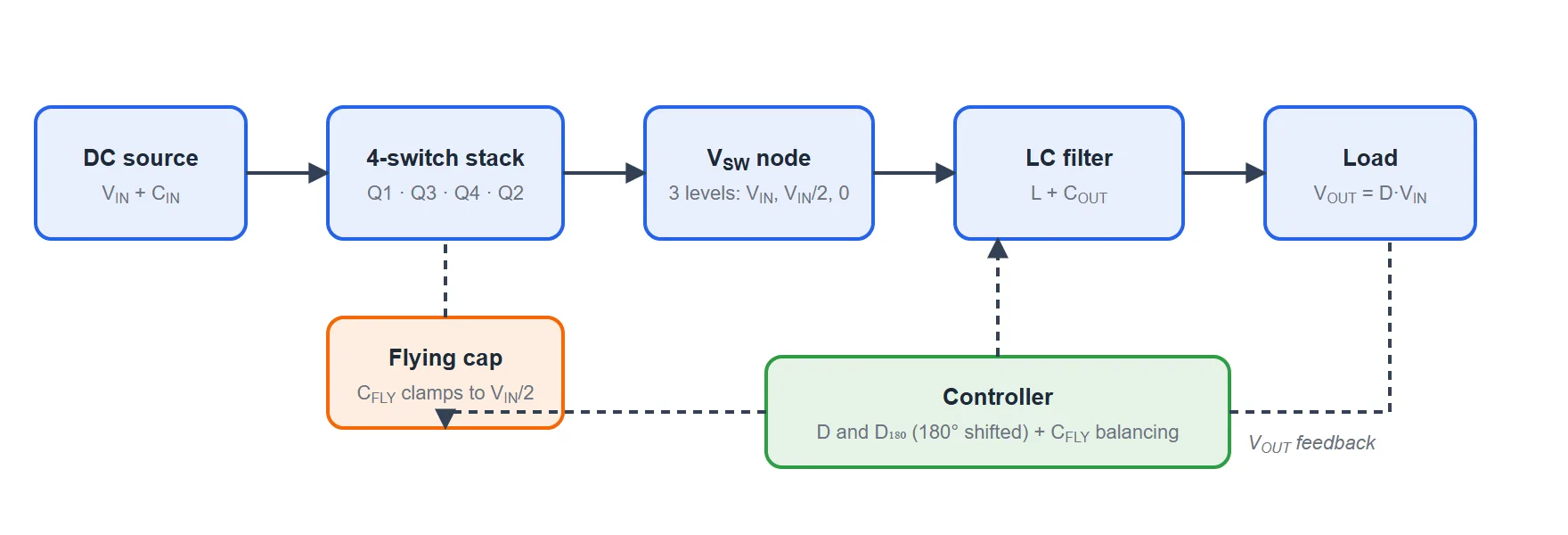
Before looking at transistors, here is the shape of the whole converter. Compared with a two-level buck, the two new blocks are the flying capacitor hanging off the switch stack and the extra job the controller has to do — it now regulates CFLY's voltage as well as the output voltage.
Circuit Diagram & Construction
The power stage is easier to read than it first looks. Take a normal buck half-bridge and split each of its two switches into two, giving a stack of four transistors in series from VIN down to ground. Reading from the top: Q1, Q3, Q4, Q2.
- The junction between Q1 and Q3 is the upper inner node — call it A.
- The junction between Q4 and Q2 is the lower inner node — call it B.
- The flying capacitor CFLY is connected across those two inner nodes, from A to B. It is not tied to ground or to VIN at either end — hence "flying".
- The switching node VSW is the middle of the stack, between Q3 and Q4. The inductor hangs off it, exactly as in a normal buck.
Everything to the right of VSW — the inductor, the output capacitor and the load — is unchanged from an ordinary buck. All the novelty is on the left.
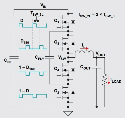
Compare the parts count with a two-level buck: two extra FETs and one extra capacitor. That is the entire cost of admission.
Gate-Drive Scheme
The gate drive is what makes the circuit a three-level converter rather than just four transistors in a row. It is built from two complementary pairs:
- Q1 and Q2 form the outer pair. Q1 is driven with duty ratio D and Q2 with 1 − D, so exactly one of them is on at any moment — just like a normal buck.
- Q3 and Q4 form the inner pair, driven with the same duty ratio D, but phase-shifted by 180° from the outer pair. Q3 gets D180 and Q4 gets 1 − D180.
The duty ratio itself is the familiar buck relationship, D = VOUT/VIN. Nothing about the control law changes. What changes is that the 180° shift means Q1 and Q3 are never in step, and it is the overlap pattern between the two pairs that produces the three levels.
Two consequences fall straight out of that shift, and both matter:
- Each transistor still turns on only once per period T. But because the two pairs are half a period apart, the switching node changes level twice per period. The frequency seen by the inductor is double the frequency seen by any transistor — written as TSW-2L = 2 × TSW-3L.
- Whether Q1 and Q3 overlap depends entirely on D. Below D = 0.5 they never overlap; above D = 0.5 they must. That is why the converter has two visibly different operating regimes, covered below.
The Flying Capacitor — Why VIN/2?
Everything in this topology rests on one assumption: CFLY sits at VIN/2. It is worth seeing why that is not an arbitrary choice but a natural resting point.
Look ahead to the modes. There are exactly two states in which current flows through the flying capacitor. In one of them (Q1 + Q4) the inductor current flows into CFLY's positive plate and charges it. In the other (Q3 + Q2) the current flows out of the positive plate and discharges it. Because both pairs are driven with the same duty ratio D, those two states last for exactly the same length of time in every cycle. Same current, same duration, opposite directions — so the net charge moved per cycle is zero, and the capacitor voltage naturally settles and stays put.
It settles at half the input because that is the balance point of the stack. With VFLY = VIN/2, node A sits VIN/2 above node B, and the four transistors share the input voltage evenly. You can verify it state by state — in every one of the four modes, each of the four transistors blocks exactly VIN/2 and never more.
Once VFLY = VIN/2 is established, the three levels appear immediately:
| Switches on | VSW equals |
|---|---|
| Q1 + Q3 (both upper) | VIN — the node is tied straight to the input |
| Q1 + Q4 | VIN − VFLY = VIN/2 |
| Q3 + Q2 | VFLY = VIN/2 |
| Q2 + Q4 (both lower) | 0 — the node is tied straight to ground |
Notice that the middle level is reached two different ways. That redundancy is not a quirk — it is precisely the mechanism that keeps the capacitor balanced, because one route charges it and the other discharges it.
Modes of Operation
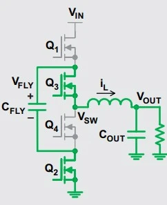
The converter only ever sits in one of four switching states. Each diagram below shows the same circuit with the conducting transistors highlighted in green, the blocking ones dashed and greyed, and the actual current path traced in orange. The inductor current is assumed continuous throughout.
Read the four modes as two pairs. Modes 1 and 3 both put VIN/2 on the switching node but do opposite things to the flying capacitor. Modes 2 and 4 are the extremes — ground and full input — and leave the flying capacitor untouched.
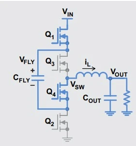
VSW = VIN/2 — the flying capacitor charges
Q1 connects the top of the stack to VIN, and Q4 connects the bottom inner node B up to the switching node. Q3 and Q2 are off. The only way through the circuit is via the flying capacitor: current leaves VIN, passes through Q1 into node A, flows down through CFLY to node B, comes back up through Q4 to VSW, and out through the inductor to the load.
Because the capacitor is in series with the path, the switching node ends up one capacitor-voltage below the input: VSW = VIN − VFLY = VIN/2. Current entering the positive plate means CFLY is charging in this mode. Q3 and Q2 each block VIN/2.
VSW = 0 — freewheeling
Both lower transistors are on and both upper ones are off. Q4 and Q2 in series form an uninterrupted path from the switching node to ground, so VSW = 0. This is exactly the freewheeling state of an ordinary synchronous buck: the inductor, which cannot change its current instantly, drives current out to the load and pulls its return path up through Q2 and Q4 from ground.
The flying capacitor is isolated here — with Q1 and Q3 both off, no current can reach node A, so CFLY simply holds whatever charge it had. The inductor current falls, since VSW = 0 is below VOUT. This mode only appears when the duty ratio is below 0.5.
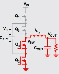
VSW = VIN/2 — the flying capacitor discharges
Now the other diagonal conducts. Q2 ties node B to ground, which drags the flying capacitor's negative plate down to 0 V. Its positive plate — node A — therefore sits at exactly VFLY above ground, and Q3 passes that straight to the switching node: VSW = VFLY = VIN/2.
The switching node is at the same level as in Mode 1, but the capacitor is doing the opposite job. Current now leaves the positive plate, flows through Q3 and the inductor to the load, and returns from ground through Q2 into the negative plate — so CFLY is discharging. Q1 and Q4 each block VIN/2.
This is the pairing that makes the whole topology work. Mode 1 and Mode 3 deliver an identical VSW to the inductor, so the load cannot tell them apart, while the flying capacitor is topped up in one and drained in the other by an equal amount.
VSW = VIN — full input applied
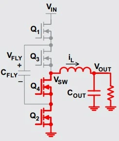
Both upper transistors conduct, putting Q1 and Q3 in series as a direct short from the input to the switching node. VSW = VIN, and the inductor current rises hard. This is the high-side-on state of an ordinary buck.
As in Mode 2, the flying capacitor is isolated — Q4 and Q2 are both off, so node B is floating and no current can pass through CFLY. This mode only appears when the duty ratio is above 0.5, because that is the only way the 180°-shifted Q1 and Q3 signals can overlap.
The four modes at a glance
| Mode | On | Off | VSW | CFLY | Inductor current | Appears when |
|---|---|---|---|---|---|---|
| 1 | Q1, Q4 | Q3, Q2 | VIN/2 | Charging | Rises if VIN/2 > VOUT, else falls | Always |
| 2 | Q2, Q4 | Q1, Q3 | 0 | Isolated | Falls | Only if D < 0.5 |
| 3 | Q3, Q2 | Q1, Q4 | VIN/2 | Discharging | Rises if VIN/2 > VOUT, else falls | Always |
| 4 | Q1, Q3 | Q4, Q2 | VIN | Isolated | Rises | Only if D > 0.5 |
Modes 1 and 3 are always present — they are the two halves of the flying capacitor's charge balance and cannot be skipped. What changes with duty ratio is only which extreme mode fills the gaps between them.
The Complete Switching Cycle
Because Q1 and Q3 carry the same duty ratio but sit half a period apart, whether they overlap is decided purely by D. That splits the converter's behaviour into two regimes.
Case 1 — Duty ratio below 0.5 (VIN > 2VOUT)
With D < 0.5, Q1 and Q3 are each on for less than half a period, so being 180° apart they can never overlap. Mode 4 is impossible. But Q2 and Q4 — each on for more than half a period — must overlap, so Mode 2 appears twice. One full period runs:
The switching node therefore toggles between VIN/2 and 0. The inductor never sees the full input voltage at all — its maximum is half of it. This is the regime where the topology's advantage is most obvious.
Case 2 — Duty ratio above 0.5 (VIN < 2VOUT)
Above 0.5 the situation inverts. Q1 and Q3 are each on for more than half a period, so they are forced to overlap — Mode 4 appears twice per period. Meanwhile Q2 and Q4 can no longer overlap, so Mode 2 disappears entirely:
Now the switching node toggles between VIN and VIN/2. The swing is still only VIN/2 — it has just moved up to sit on top of the middle level instead of underneath it. Notice that Modes 1 and 3 survive in both regimes, which is what keeps the flying capacitor balanced no matter which side of 0.5 the converter is running on.
Case 3 — Exactly D = 0.5
At precisely 50 % duty something neat happens. Q1 and Q4 are on for one half of the period, Q3 and Q2 for the other half, and nothing else ever occurs. The switching node never leaves VIN/2 — and since D = 0.5 means VOUT = VIN/2, the switching node is sitting at exactly the output voltage.
With no voltage across the inductor, there is nothing to drive a current change, so the ripple current falls to zero. A two-level buck at D = 0.5 is at its worst ripple; the three-level buck at the same point has none at all. The two topologies are exact opposites there.
Waveforms Explained in Detail
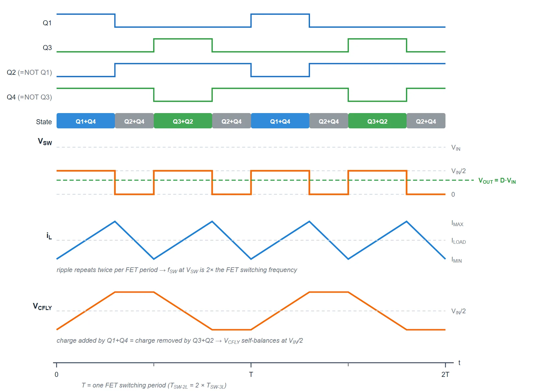
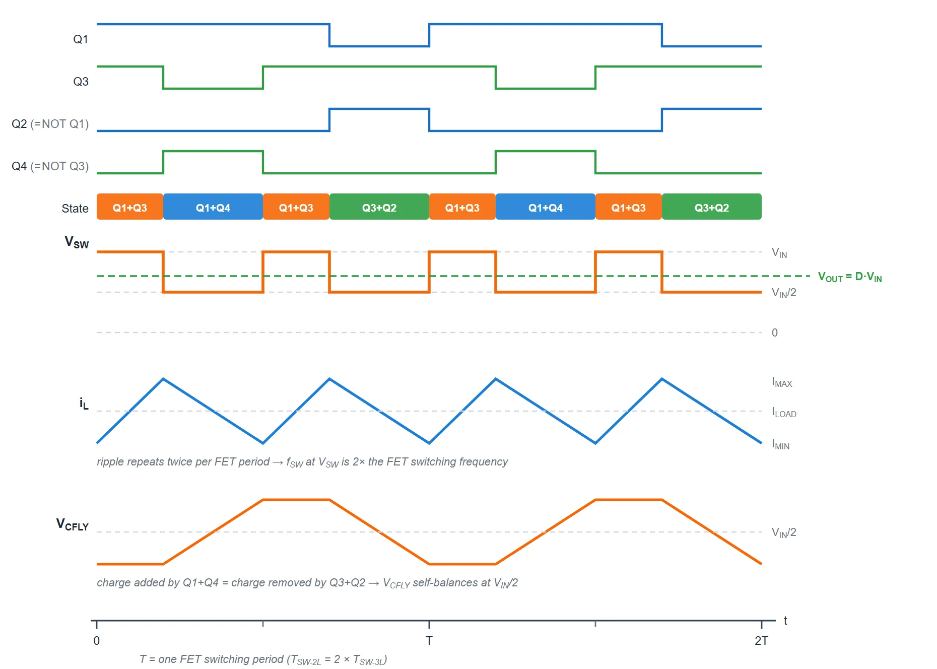
These are the waveforms that tie everything above together. Each set stacks eight synchronised traces on one time axis: the four gate signals, the resulting mode, the switching node, the inductor current and the flying capacitor voltage. The horizontal axis is marked in units of T, one transistor switching period — watch how often things happen inside a single T.
Waveform set 1 — D = 0.3 (below half duty)
Reading it trace by trace
- Q1 and Q3 gates: identical pulses of width 0.3T, but Q3's pulse starts half a period after Q1's. Because 0.3 + 0.3 < 1, the two pulses never touch — this is the visual proof that Mode 4 cannot exist below half duty.
- Q2 and Q4 gates: simply the inverses of Q1 and Q3. They are on for 0.7T each, so they overlap heavily — and every one of those overlaps is a Mode 2 (0 V) interval.
- State band: the cycle reads Q1+Q4 → Q2+Q4 → Q3+Q2 → Q2+Q4. The two VIN/2 intervals are equal in width, which is the charge balance made visible.
- VSW: a square wave between VIN/2 and 0 — never reaching VIN. Crucially it completes two full pulses inside one period T, while every individual transistor switched only once. The green dashed line is the average, which is what the LC filter delivers: VOUT = D·VIN = 0.3 VIN.
- iL: the familiar triangle, but with two ripple cycles per transistor period instead of one. It rises whenever VSW is above VOUT (here VIN/2 > 0.3VIN) and falls whenever it is below. The peak-to-peak swing is small for two compounding reasons: the driving voltage is only VIN/2 − VOUT instead of VIN − VOUT, and it only gets 0.3T to act instead of a full half-cycle.
- VCFLY: ramps up during Q1+Q4, sits flat while the capacitor is isolated, ramps down by the same amount during Q3+Q2, sits flat again. It ends each period exactly where it started — that closed loop is the self-balancing mechanism. The ramp is small compared with the VIN/2 it rides on; the trace is magnified here to make it readable.
Waveform set 2 — D = 0.7 (above half duty)
What changed, and what did not
- The gates now overlap. Q1 and Q3 are each on for 0.7T. Two pulses that wide, half a period apart, cannot avoid each other — so Q1+Q3 (Mode 4) appears twice per period. Meanwhile Q2 and Q4, on for only 0.3T each, never meet, so the 0 V state has vanished completely.
- VSW has moved up a level — it now swings between VIN and VIN/2. The size of the swing is unchanged at VIN/2; only its position moved. This is why the inductor benefit survives on both sides of 0.5.
- iL still ripples twice per period. The doubled effective frequency has nothing to do with duty ratio — it comes purely from the 180° phase shift, so it is always there.
- VCFLY still closes its loop. Charging happens during Q1+Q4 and discharging during Q3+Q2, exactly as before. The isolated intervals are now Mode 4 instead of Mode 2, but the capacitor cannot tell the difference — either way, no current flows through it.
- The average is still D·VIN. The node spends 2(D − 0.5) of the period at VIN and the remainder at VIN/2, and those weights work out to exactly 0.7 VIN. The control law never changed.
Why the Inductor Shrinks to One-Quarter
This is the headline claim, so it is worth deriving rather than asserting. Ripple current in any inductor comes from the same relationship, V = L·di/dt, rearranged as ΔiL = VL × Δt / L. So we only need the voltage across the inductor and how long it is applied.
Two-level buck. While the high-side FET is on, the inductor sees VIN − VOUT for a time D·T. With VOUT = D·VIN:
That peaks at D = 0.5, where D(1 − D) = 0.25.
Three-level buck, D < 0.5. The inductor sees VIN/2 − VOUT for a time D·T (the Mode 1 interval). Substituting VOUT = D·VIN gives a driving voltage of VIN(0.5 − D):
Working the same way above half duty (the inductor sees VIN − VOUT for (D − 0.5)T) gives VIN(1 − D)(D − 0.5)·T/L. Both halves collapse into one expression if we write u = |D − 0.5|:
That expression is largest at u = 0.25 — that is, at D = 0.25 or D = 0.75 — where it equals 0.0625. Compare the two peaks:
So for the same inductance and the same transistor switching frequency, the three-level buck's worst-case ripple is a quarter of the two-level buck's. Turn that around: accept the same ripple your two-level design already tolerated, and the inductance can drop to L3L = L2L/4 — which in practice means a physically smaller part, a cheaper part, or a part with lower DC resistance in the same footprint.
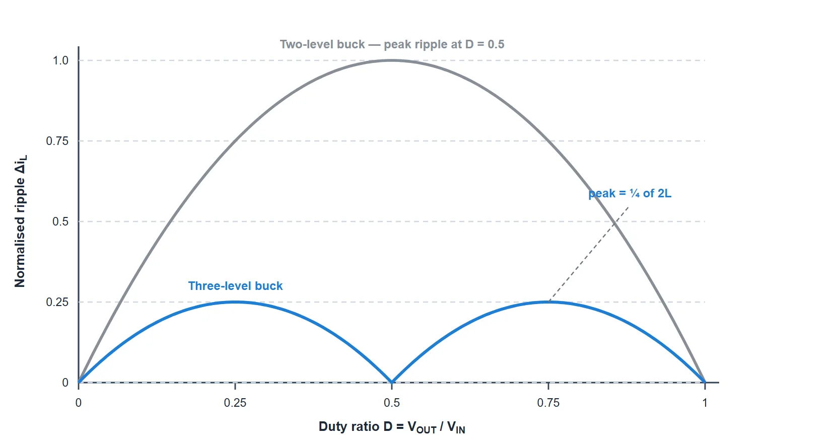
The chart makes the character of the two topologies plain. The two-level buck has a single hump peaking exactly in the middle. The three-level buck has two smaller humps with a zero between them, peaking at a quarter of the two-level maximum, and it collapses to zero ripple at D = 0, 0.5 and 1. If your application happens to live near 50 % duty — a 2S battery from a 9 V adapter, say — the improvement is far better than 4×.
Key Formulas
Throughout, D = VOUT/VIN, fSW is the switching frequency of an individual transistor (so the switching node runs at 2fSW), ILOAD is the output current, and K is the allowed ripple as a fraction of ILOAD — typically 0.2 to 0.4.
| Quantity | Formula |
|---|---|
| Output voltage | VOUT = D × VIN |
| Switch-node levels | VIN, VIN/2, 0 |
| Flying-capacitor voltage | VFLY = VIN/2 |
| Voltage across each FET | VIN/2 (in every state) |
| Switch-node frequency | 2 × fSW, i.e. TSW-2L = 2 × TSW-3L |
| Inductor ripple (2L, for reference) | ΔiL = VIN × D(1−D) / (L × fSW) |
| Inductor ripple (3L) | ΔiL = VIN × (0.5u − u²) / (L × fSW), u = |D−0.5| |
| Required inductance (3L) | L = VIN × (0.5u − u²) / (K × ILOAD × fSW) |
| Inductance ratio at worst case | L3L = L2L / 4 |
| CFLY ripple voltage | ΔVCFLY = ILOAD × (0.5 − u) / (CFLY × fSW) |
| CFLY RMS current | ICFLY(RMS) = √[ 2(0.5 − u) × (ILOAD² + ΔiL²/12) ] |
| Inductor DCR loss | PDCR = (ILOAD² + ΔiL²/12) × RDCR |
Two of these deserve a comment. The CFLY ripple voltage is largest at D = 0.5 — exactly where the inductor ripple is zero — because that is where the capacitor carries the full load current for the longest. The topology's best point for the inductor is its worst point for the flying capacitor. And the DCR loss expression shows why ripple barely matters for conduction loss: the ΔiL²/12 term is tiny next to ILOAD², so a low-DCR inductor beats a low-ripple one.
Sizing rule of thumb for the flying capacitor: pick CFLY so that ΔVCFLY stays under about 10 % of VIN/2, or the control loop starts to suffer. Remember to apply ceramic derating for DC bias and temperature before you believe the number on the part — and check the RMS current rating, because at D = 0.5 that capacitor is carrying the full load current.
Losses — Three-Level vs Two-Level
A fair loss comparison needs a fair basis, so fix the total silicon area and let the topology divide it up. In the three-level converter the area that the two-level buck gave to its single high-side FET is now split between Q1 and Q3. Because those two only have to block VIN/2, a half-area FET at half the voltage rating ends up with about the same on-resistance as the original — so the stack has twice the total resistance in the current path. The same reasoning applies to the low side.
Working through the loss terms on that basis:
| Loss term | What it is | 3L vs 2L | Why |
|---|---|---|---|
| PCOND | I²R in the switches | ×2 | Two FETs in series in the path instead of one, each with the same resistance |
| PDT | Body-diode loss during dead time | ×2 | Two body diodes conduct in series instead of one |
| PIV | Overlap of V and I during transitions | ×½ | Half the voltage, and at the same dv/dt the transitions take half as long |
| POSS | Output-capacitance charge loss | ×½ | Same total stored charge, but discharged from half the voltage |
| PGATE | Gate-drive charge | ×1 | Four half-size gates draw the same total charge as two full-size ones |
| PQRR | Body-diode reverse recovery | ×1 | Twice as many recovery events, each at half the voltage |
So the three-level buck is not a free lunch on silicon: it trades conduction loss for switching loss. Conduction and dead-time losses double while the two voltage-dependent switching terms halve.
That trade is a good one, and the reason is worth understanding. Conduction loss falls as you add FET area; switching loss rises with it. Total on-chip loss is therefore a U-shaped curve, minimised where the two are equal. Because the three-level topology starts with lower switching loss, its optimum sits at a larger die area than the two-level's — you can afford to spend more silicon buying down conduction loss before switching loss catches up.
And this on-chip accounting is only part of the story. It deliberately holds the inductor constant, which throws away the topology's main prize. In a real design you would cash in the 4× ripple headroom for a smaller, lower-DCR inductor — and since DCR loss usually dominates the total in a compact converter, that is where the real efficiency win lands. If DCR scales with inductance, a quarter of the inductance means roughly a quarter of the inductor loss.
Flying-Capacitor Balancing (the hard part)
Every benefit on this page has been quietly resting on one assumption: VFLY = VIN/2. It is worth being blunt about what happens when that assumption breaks, because this — not the extra parts — is what makes three-level converters genuinely difficult to build.
If the flying capacitor drifts off VIN/2, the three levels stop being evenly spaced. The switching node lands at VIN − VFLY in Mode 1 and at VFLY in Mode 3, and those are no longer the same number. Two things then go wrong at once:
- The transistors lose their voltage protection. The VIN/2 rating that justified using low-voltage FETs was a consequence of balance. If VFLY collapses toward zero, some FET in the stack has to block close to the full VIN — and it was not chosen to survive that.
- The ripple benefit evaporates. Unequal levels mean the inductor sees an alternating pair of different voltages, reintroducing a beat at the original frequency. The 4× advantage degrades.
The natural charge balance described earlier is real, but it is only a steady-state argument, and it is weak — it relies on the charging and discharging intervals being equal, which stops being true exactly when you need it most:
- Start-up, when CFLY begins at 0 V and there is no balance to maintain yet.
- Load transients, when the duty ratio moves faster than the capacitor can follow.
- Light load, where there is barely any current to move charge with, and leakage can win.
- D approaching 100 %, where the balancing states shrink toward zero width.
Real three-level controllers therefore add active balancing circuitry that measures VFLY — often indirectly, by watching the switching node — and nudges the two duty ratios apart very slightly to steer the capacitor back. Commercial parts treat that circuitry as proprietary, and it is a large part of why you buy a three-level converter IC rather than build one from discrete FETs.
Three-Level vs Two-Level Buck
| Feature | Two-Level (Synchronous) Buck | Three-Level (Flying-Cap) Buck |
|---|---|---|
| Transistors | 2 | 4 |
| Capacitors | CIN, COUT | CIN, COUT, CFLY |
| VSW levels | VIN, 0 | VIN, VIN/2, 0 |
| FET voltage stress | VIN | VIN/2 |
| Frequency at VSW | fSW | 2 × fSW |
| Worst-case ripple | Peaks at D = 0.5 | Quarter of 2L; zero at D = 0.5 |
| Inductance for same ripple | L | L / 4 |
| Conduction loss (same die area) | Baseline | About double |
| Voltage-dependent switching loss | Baseline | About half |
| Control complexity | One voltage loop | Voltage loop + CFLY balancing |
| Behaviour at D = 0.5 | Worst ripple | Zero ripple |
| Best suited to | General-purpose step-down | High VIN/VOUT ratio, tight space, high power density |
A Real-World Example
Theory is one thing; here is what the topology actually delivered in a shipping product. TI compared two of its own single-cell battery chargers in similar packages — the BQ25910, a three-level part, against the BQ25898, a conventional two-level one.
The first thing to notice is that the three-level part runs at 750 kHz against the two-level part's 1.5 MHz — half the switching frequency — and still uses a smaller inductor: 470 nH against 1 µH. That is a 2× reduction rather than the theoretical 4×, which is a useful reminder that real designs spend some of the headroom on other goals.
Board area, comparing like-for-like components and excluding routing:
| Charger | IC | Inductor | CFLY | CBAT | CAUX | Total |
|---|---|---|---|---|---|---|
| BQ25898 (2L) | 7.0 | 17.6 | — | 1.3 | — | 25.9 mm² |
| BQ25910 (3L) | 5.9 | 5.5 | 2.6 | — | 0.5 | 16.5 mm² (−36 %) |
Look at where the saving comes from: the inductor drops from 17.6 mm² to 5.5 mm². Even after paying 2.6 mm² for the flying capacitor it was not close. The inductor was the problem, and shrinking it was the whole point.
Measured at 9 V in, a 3.8 V battery and 3 A of charge current, the two-level part managed 89.3 % efficiency and the three-level part 93.2 % — a 3.9-point gain, which is about a 36 % cut in total loss. Framed the way a thermally-limited designer would care about: for a 1.5 W loss budget, the two-level charger delivers 3.2 A while the three-level delivers 4.2 A — 31 % more current in 36 % less area.
Advantages & Disadvantages
Advantages
- Much smaller inductor — a quarter of the inductance for the same ripple, which is usually the largest component on the board.
- Half the voltage stress on every FET, allowing faster, cheaper, lower-RDS(on) devices.
- Double the effective frequency at the inductor without any transistor switching faster, so no extra switching loss is paid for it.
- Lower switching losses — the voltage-dependent terms roughly halve.
- Zero ripple at D = 0.5, precisely where a two-level buck is at its worst.
- Higher power density — measurably smaller solution size at higher output current.
Disadvantages
- Flying-capacitor balancing is genuinely hard, and a failure to balance can destroy the transistors rather than merely degrade performance.
- More components — two extra FETs and a flying capacitor that must handle full load current at D = 0.5.
- Roughly double the conduction loss for the same silicon area, since two FETs sit in series in the current path.
- More complex gate drive, including a floating drive for the inner devices.
- Harder start-up, because the flying capacitor must be pre-charged before normal switching can safely begin.
- Least benefit at extreme duty ratios, where the balancing intervals shrink.
Applications
- Fast battery chargers in phones, tablets and wearables — high-voltage USB Type-C adapters stepping down to a single-cell battery, in almost no space.
- Point-of-load and VRM rails in laptops and servers, where a 12 V bus must reach 1 V at high current — a large step-down ratio that suits the topology well.
- Envelope tracking for RF power amplifiers, which needs a fast-moving supply rail that a small inductor makes possible.
- High-voltage industrial DC-DC, where halving the FET voltage stress allows lower-voltage, better-performing devices.
- Automotive and 48 V systems, where board area and thermal budget are both tight.
- USB Power Delivery front-ends handling wide input ranges in compact adapters.
The pattern is consistent: the topology earns its extra complexity wherever the input-to-output ratio is large and space or heat is the binding constraint. For a gentle step-down in a roomy design, a plain two-level buck is still the right answer.