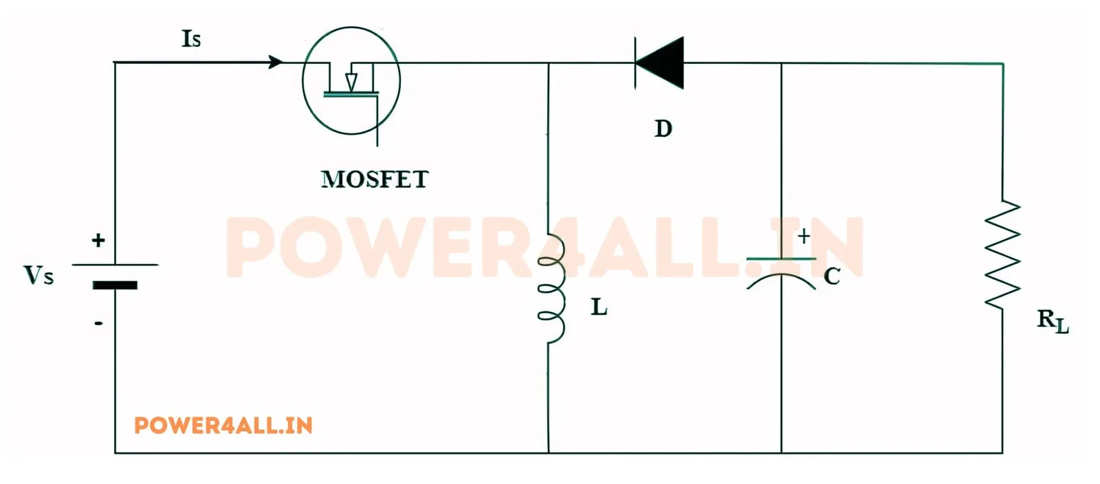
What is an inverting buck-boost converter?
A buck-boost converter is a switched-mode DC-DC converter whose output can be either lower or higher than the input, and whose polarity is inverted (negative). A single inductor is charged from the input through a MOSFET; when the switch opens, the inductor discharges through a diode into the output capacitor with the opposite polarity. It combines the ranges of the buck and the boost in one topology.
How it works — the two switching states
- Switch ON (0 → D·T): the MOSFET connects the inductor across the input; the current ramps up as
diL/dt = Vin/L, storing energy. The diode is reverse-biased, so the output capacitor alone supplies the (negative) load. - Switch OFF (D·T → T): the inductor forces its current through the diode into the output capacitor with reversed polarity; the current ramps down as
diL/dt = −|Vo|/L, and the output is negative.
Key equations
This simulator does not plug numbers into these formulas — it numerically integrates the real switching circuit (with your device parasitics) to steady state, then measures Vo, the ripple and the losses from the resulting waveforms and compares them to the equations above in the accuracy panel.
Step-up or step-down?
Because |Vo| = D·Vin/(1 − D), the converter steps the magnitude down for D < 0.5, gives |Vo| = Vin at D = 0.5, and steps up for D > 0.5 — always with an inverted output. Use the Step-down and Step-up presets to see both.
CCM / DCM & device stress
As with the buck and boost, at light load or with a small inductor the current becomes discontinuous (DCM) and the output magnitude rises above the ideal. Note that the inductor carries the sum of the input and output currents, and the switch and diode block Vin + |Vo| — the highest stress of the three basic topologies. The loss-breakdown chart shows where the power goes.
Buck vs boost vs buck-boost
| Converter | Output vs input | Ideal Vo |
|---|---|---|
| Buck | Steps down (Vo < Vin) | D·Vin |
| Boost | Steps up (Vo > Vin) | Vin/(1 − D) |
| Buck-Boost | Up or down, inverted | −D·Vin/(1 − D) |
Applications
Generating a negative rail (e.g. −5 V / −12 V) from a positive supply, LED drivers, battery-powered systems where the output may be above or below the battery voltage, and as the basis of the non-inverting Ćuk, SEPIC and ZETA converters.
Frequently asked questions
What is the output voltage of a buck-boost converter?
In CCM the ideal output is Vo = −D·Vin/(1 − D) — negative, and either smaller or larger than Vin depending on D.
Why is the output negative?
The inductor discharges into the output capacitor with reversed polarity during the off-time, so the output is inverted relative to the input ground.
Does it step up or step down?
|Vo| = D·Vin/(1 − D): step-down for D < 0.5, equal at D = 0.5, step-up for D > 0.5.
What is the inductor ripple current?
ΔiL = Vin·D/(L·fsw). The inductor carries both input and output current, so its average is higher than in a buck or boost.
What must the switch and diode withstand?
Both block Vin + |Vo| = Vin/(1 − D) — higher than either a buck or a boost of the same ratio.