Complete Diode Mastery Guide
Master semiconductor diodes - from fundamental PN junction physics and construction to advanced applications in rectification, voltage regulation, protection circuits, and modern power electronics
Complete Learning Path - Diode Fundamentals to Applications
Navigate through comprehensive coverage of diodes from basic PN junction physics to advanced power electronics applications
What is a Diode? The Foundation of Modern Electronics
A diode is a two-terminal semiconductor device that allows current to flow in only one direction. Formed by joining P-type and N-type semiconductor materials, diodes are the fundamental building blocks of modern electronics, enabling rectification, voltage regulation, signal processing, and protection in countless applications.

The Electronic One-Way Valve
Think of a diode as an electronic one-way valve that allows electrical current to flow easily in one direction (forward bias) while blocking current flow in the opposite direction (reverse bias), creating the foundation for rectification and switching.
Diode Analogy
- Water check valve → Allows flow in one direction only
- Forward bias → Valve open, current flows
- Reverse bias → Valve closed, blocks current
- Threshold voltage → Minimum pressure to open valve
PN Junction = P-type + N-type
Basic diode formed by joining P and N semiconductor materials
Why Diodes Are Essential
Diodes are found in virtually every electronic device, from simple power supplies to complex digital circuits. Their ability to control current direction makes them indispensable for converting AC to DC power, protecting circuits from voltage spikes, and enabling digital logic operations.
Unidirectional Conduction
Diodes allow current flow in only one direction, with typical forward voltage drops of 0.3V (germanium) to 0.7V (silicon) to 3V+ (LEDs).
Reverse Blocking
In reverse bias, diodes block current flow with only tiny leakage currents (nanoamps to microamps) until breakdown voltage is reached.
Fast Switching
Modern diodes can switch from conducting to blocking (and vice versa) in nanoseconds, enabling high-frequency applications.
Wide Voltage Range
Diodes are available for applications from millivolts to kilovolts, with current ratings from microamps to thousands of amperes.
Diode Terminals and Symbol
Two Main Terminals
- Anode: P-type side, positive terminal when forward biased
- Cathode: N-type side, negative terminal when forward biased
- Symbol: Triangle pointing toward line (anode to cathode)
- Current flow: From anode to cathode when forward biased
- Polarity: Critical for proper circuit operation
Operating States
- Forward bias: Anode positive, cathode negative - conducts
- Reverse bias: Anode negative, cathode positive - blocks
- Forward voltage: Voltage drop when conducting (0.7V typical)
- Reverse breakdown: Maximum reverse voltage before failure
- Switching time: Time to change between states
Diodes in Everyday Electronics
- Power supplies: AC to DC conversion in chargers and adapters
- LED lights: Light-emitting diodes for illumination
- Solar panels: Prevent reverse current flow
- Circuit protection: Flyback diodes in motor circuits
- Radio circuits: Demodulation and detection
- Digital logic: Gates and switching circuits
Historical Impact
The first semiconductor diode was developed in the early 1900s using crystals like galena. The invention of the silicon junction diode in the 1940s revolutionized electronics, enabling the development of transistors, integrated circuits, and all modern electronic devices we use today.
Diode Physics & PN Junction Fundamentals
Understanding diode operation requires exploring the physics of the PN junction - the boundary between P-type and N-type semiconductor materials. This junction creates unique electrical properties that enable the diode's unidirectional current flow and form the foundation of all semiconductor devices.
Semiconductor Doping and Materials
P-Type and N-Type Materials
Pure silicon becomes a semiconductor when doped with specific impurities that create either excess electrons (N-type) or electron holes (P-type), forming the basis for diode operation.
N-Type Semiconductor
- Dopant: Phosphorus, arsenic, or antimony (Group V elements)
- Extra electrons: Fifth valence electron becomes mobile
- Majority carriers: Electrons (negative charge)
- Minority carriers: Holes (positive charge)
P-Type Semiconductor
- Dopant: Boron, aluminum, or gallium (Group III elements)
- Missing electrons: Creates holes that can accept electrons
- Majority carriers: Holes (positive charge)
- Minority carriers: Electrons (negative charge)
Si + B → P-type (holes)
Si + P → N-type (electrons)
Doping creates charge carriers
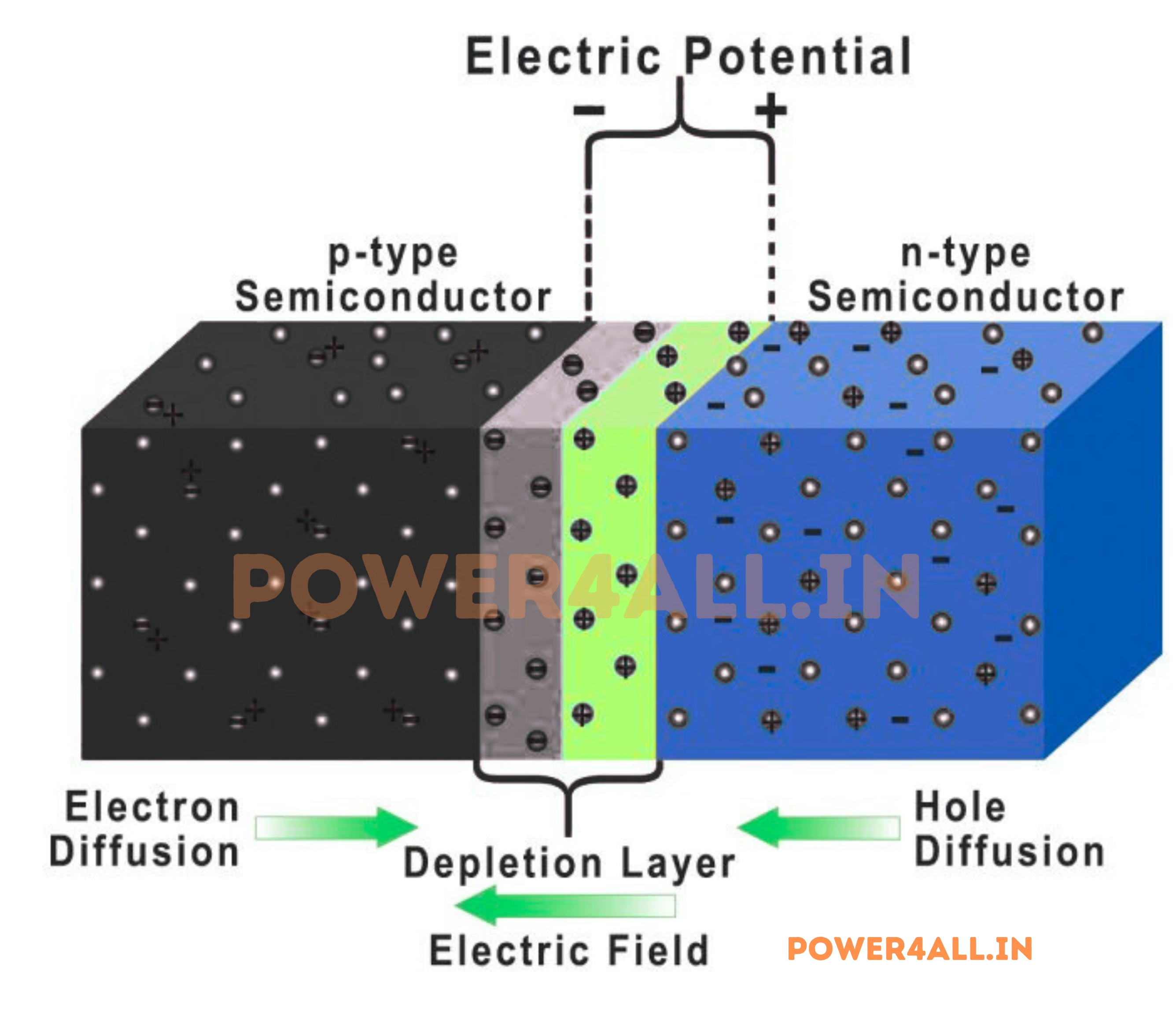
PN Junction Formation
Understanding PN Junction Physics and Depletion Region
Junction Formation Process
When P-type and N-type materials are joined, charge carriers diffuse across the boundary, creating a depletion region with built-in electric field.
Depletion Region Characteristics
| Property | Description | Typical Value | Effect |
|---|---|---|---|
| Width | Region depleted of mobile carriers | 0.1-1μm | Determines junction capacitance |
| Built-in Voltage | Internal electric field potential | 0.3-0.7V | Must be overcome for conduction |
| Electric Field | Field strength in depletion region | 10⁴-10⁶ V/cm | Controls barrier height |
| Capacitance | Junction capacitance effect | pF to nF | Affects high-frequency response |
VBI = (kT/q) × ln(NAND/ni²)
Built-in voltage based on doping concentrations
Forward and Reverse Bias Operation
Forward Bias Operation
Anode positive, cathode negative
Forward Bias Physics
- Barrier reduction: External voltage reduces depletion width
- Carrier injection: Electrons and holes cross junction
- Current flow: Exponential increase with voltage
- Voltage drop: 0.7V for silicon, 0.3V for germanium
Forward Current Equation
IF = IS(e^(VF/nVT) - 1)
Shockley diode equation
Key Parameters
- IS: Reverse saturation current
- n: Ideality factor (1-2)
- VT: Thermal voltage (kT/q ≈ 26mV at 25°C)
- VF: Forward voltage
Reverse Bias Operation
Anode negative, cathode positive
Reverse Bias Physics
- Barrier increase: Depletion region widens
- Current blocking: Only tiny leakage current flows
- Capacitance effect: Junction acts like variable capacitor
- Breakdown voltage: Maximum reverse voltage tolerated
Reverse Current Sources
- Thermal generation: Minority carrier generation
- Surface leakage: Current along crystal surface
- Tunneling: Quantum mechanical effect at high fields
- Avalanche: Impact ionization at breakdown
Breakdown Mechanisms
- Avalanche breakdown: Carrier multiplication (>6V)
- Zener breakdown: Quantum tunneling (<6V)
- Thermal breakdown: Excessive power dissipation
- Surface breakdown: High field at surface
Temperature Effects on Diode Operation
Temperature Dependencies and Thermal Considerations
Temperature Coefficients
Diode characteristics change significantly with temperature, affecting forward voltage, reverse current, and breakdown voltage.
Forward Voltage Temperature Coefficient
Forward voltage decreases by approximately -2mV/°C for silicon diodes. This negative temperature coefficient must be considered in precision circuits.
Reverse Current Temperature Effect
Reverse leakage current approximately doubles for every 10°C temperature increase, following exponential relationship with temperature.
Breakdown Voltage Variation
Zener diodes have positive or negative temperature coefficients depending on breakdown mechanism. Avalanche breakdown has positive tempco.
| Parameter | Temperature Coefficient | Effect | Compensation Methods |
|---|---|---|---|
| Forward Voltage | -2mV/°C | Lower VF at high temperature | Temperature compensation circuits |
| Reverse Current | ×2 per 10°C | Exponential increase | Thermal management, cooling |
| Zener Voltage | ±0.05-0.1%/°C | Voltage regulation drift | Temperature compensated references |
| Switching Speed | Faster at high temp | Reduced carrier lifetime | Circuit timing adjustments |
Temperature Compensation Techniques
- Thermistors: Use opposite temperature coefficient
- Bandgap references: Temperature-independent voltage references
- Thermal coupling: Match thermal environments
- Digital compensation: Software correction in microcontroller systems
Quantum Effects
At very small dimensions and high electric fields, quantum mechanical effects like tunneling become significant in diode operation. This is exploited in tunnel diodes and is a limiting factor in scaling semiconductor devices to nanometer dimensions.
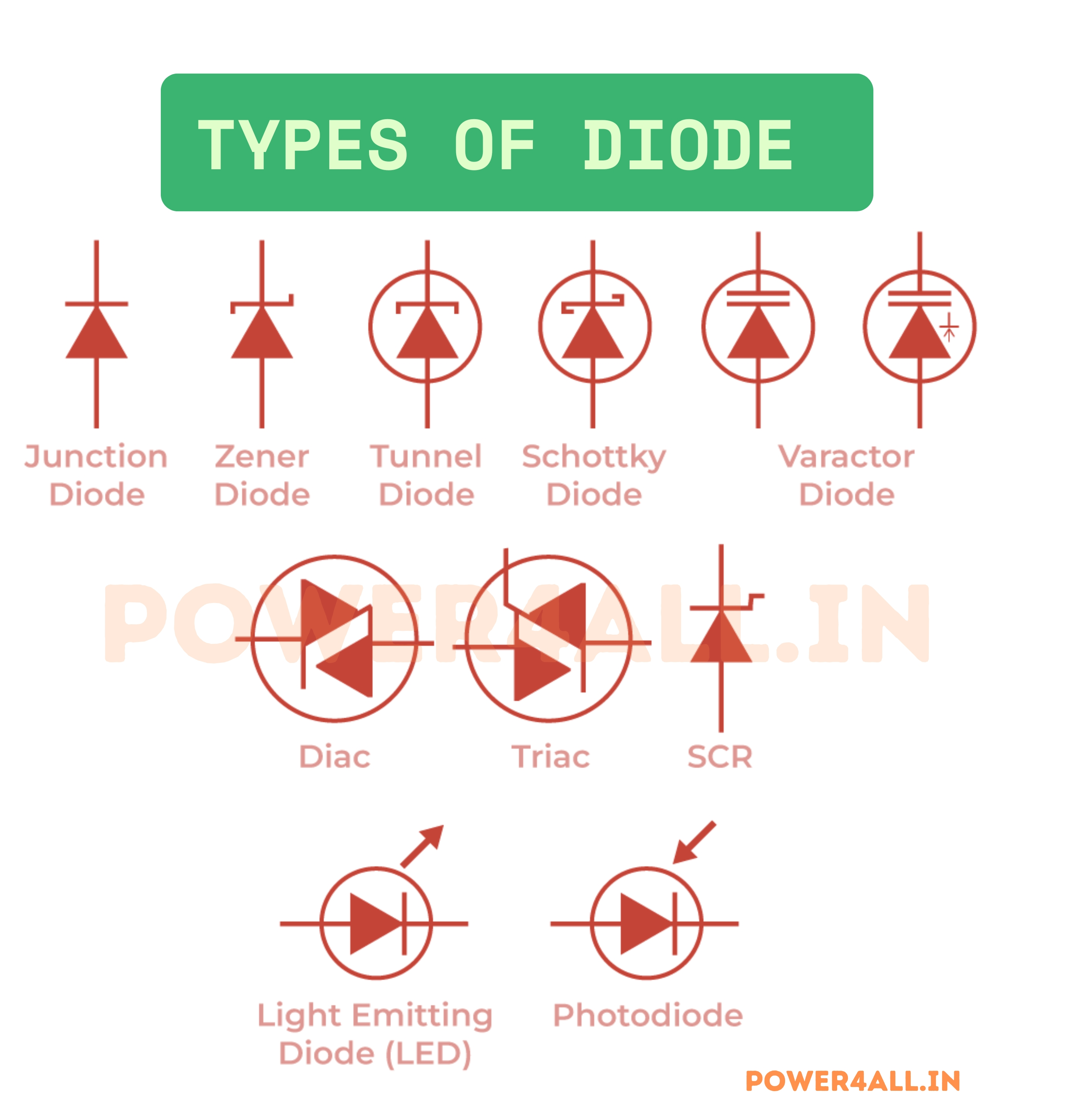
Types of Diodes and Classifications
Diodes come in many specialized types, each optimized for specific applications. From simple rectifier diodes to sophisticated light-emitting and voltage-regulating devices, understanding the different types helps in selecting the optimal diode for any circuit requirement.
Rectifier Diodes
Standard Rectifier Diodes
AC to DC conversion applications
Key Characteristics
- Forward voltage: 0.7V (silicon), 0.3V (germanium)
- Current ratings: 1A to 3000A
- Voltage ratings: 50V to 10kV+
- Recovery time: 1-100μs typical
Common Series
- 1N400x series: 1A, 50V-1000V (1N4001-1N4007)
- 1N540x series: 3A, 50V-600V general purpose
- 6A series: 6A automotive and industrial
- High voltage: Specialized high-voltage rectifiers
Applications
- Power supplies: Linear and switching regulators
- Battery chargers: DC power conversion
- Motor drives: DC bus rectification
- Automotive: Alternator rectification
Fast Recovery Diodes
High-frequency switching applications
Enhanced Characteristics
- Recovery time: 50ns to 500ns
- Soft recovery: Reduced EMI and stress
- Low stored charge: Minimal reverse current
- Temperature stable: Consistent performance
Construction Features
- Lifetime control: Gold or platinum doping
- Epitaxial structure: Optimized carrier profiles
- Guard rings: High voltage capability
- Low capacitance: High-frequency performance
Applications
- Switching power supplies: Flyback and forward converters
- Motor drives: PWM inverters and rectifiers
- UPS systems: High-frequency conversion
- Induction heating: RF power applications
Voltage Regulation Diodes
Zener Diodes
Voltage regulation and reference
Operating Principle
- Reverse breakdown: Controlled avalanche or Zener effect
- Constant voltage: Stable voltage across wide current range
- Voltage range: 2.4V to 200V available
- Power ratings: 250mW to 50W
Breakdown Mechanisms
- Zener breakdown: <6V, negative temperature coefficient
- Avalanche breakdown: >6V, positive temperature coefficient
- Combination: 6V region has near-zero tempco
- Temperature compensation: Series-connected types
Applications
- Voltage regulation: Simple shunt regulators
- Reference voltage: ADC and DAC references
- Overvoltage protection: Clamp circuits
- Level shifting: Digital logic interfaces
Transient Voltage Suppressors
ESD and surge protection
Protection Characteristics
- Fast response: Picosecond clamping time
- High surge current: Hundreds of amperes
- Low clamping voltage: Precise protection levels
- Bidirectional types: AC line protection
TVS Types and Ratings
- Unidirectional: DC applications, asymmetric protection
- Bidirectional: AC applications, symmetric protection
- Voltage range: 5V to 440V working voltages
- Power ratings: 400W to 30kW peak pulse power
Applications
- ESD protection: USB, HDMI, and data interfaces
- Automotive: Load dump and ignition transients
- Telecom: Lightning and switching surge protection
- Industrial: Motor drive and power supply protection
Signal and Switching Diodes
Small Signal Diodes
Low current, high-frequency applications
Key Features
- Low capacitance: 1-4pF typical
- Fast switching: 1-10ns recovery time
- Low current: 10-200mA maximum
- Small packages: SOD-323, SOD-523, DO-35
Common Types
- 1N4148: Universal switching diode, 100V 200mA
- 1N914: Fast switching, computer logic
- BAV99: Dual series diode in SOT-23
- 1N5711: Schottky detector diode
Applications
- Logic circuits: Digital switching and clamping
- RF detection: Radio and communication systems
- Voltage multipliers: High-voltage generation
- Protection circuits: Low-power ESD protection
Schottky Diodes
Low forward drop, fast switching
Unique Characteristics
- Metal-semiconductor junction: No PN junction
- Low forward voltage: 0.15-0.45V typical
- Zero recovery time: No stored charge
- Higher leakage: Temperature-dependent reverse current
Construction Materials
- Silicon Schottky: Most common, 0.3-0.5V forward drop
- Gallium Arsenide: Ultra-low forward drop, high frequency
- Silicon Carbide: High temperature, high voltage
- Metal contacts: Platinum, tungsten, molybdenum
Applications
- Power supplies: Low-voltage, high-efficiency rectification
- RF circuits: Mixing, detection, and switching
- Solar systems: Bypass and blocking diodes
- Battery circuits: Reverse polarity protection
Optoelectronic Diodes
Light-Emitting Diodes (LEDs)
Electroluminescent semiconductor devices
LED Materials and Colors
- GaAs: Infrared (850-940nm)
- GaAsP: Red (630-700nm)
- GaP: Green (520-570nm)
- GaN: Blue (450-490nm), White (phosphor-converted)
- InGaN: High-efficiency blue and white
LED Characteristics
- Forward voltage: 1.8V (red) to 3.5V (blue/white)
- Efficiency: 100-200 lumens/watt for high-power types
- Lifetime: 50,000+ hours typical
- Temperature effects: Efficiency decreases with heat
Applications
- General lighting: Residential and commercial illumination
- Automotive: Headlights, taillights, signals
- Displays: Digital signs, TV backlighting
- Indicators: Status lights and panel indicators
Photodiodes
Light-sensing semiconductor devices
Operating Principles
- Photovoltaic mode: Generates voltage from light
- Photoconductive mode: Current proportional to light
- Reverse bias operation: Linear response, low dark current
- Spectral response: Wavelength-dependent sensitivity
Photodiode Types
- Silicon: 400-1100nm, general purpose
- Germanium: 800-1700nm, near-infrared
- InGaAs: 900-2500nm, fiber optic communications
- Avalanche (APD): Internal gain, high sensitivity
Applications
- Optical communications: Fiber optic receivers
- Light meters: Photography and scientific instruments
- Safety systems: Smoke detectors, proximity sensors
- Medical devices: Pulse oximeters, optical imaging
Specialty Diodes
Advanced and Specialized Diode Types
Variable Capacitance Diodes (Varactors)
Voltage-controlled capacitors using the depletion region width variation with reverse bias voltage.
| Diode Type | Key Feature | Applications | Voltage Range |
|---|---|---|---|
| Varactor Diodes | Variable capacitance | Tuning circuits, VCOs | 1-30V |
| Tunnel Diodes | Negative resistance | Oscillators, amplifiers | 0.1-0.6V |
| PIN Diodes | Wide intrinsic region | RF switches, attenuators | 50-1000V |
| Step Recovery | Snap-off effect | Frequency multipliers | 20-200V |
High-Frequency and Microwave Diodes
Gunn Diodes
Transferred electron devices for microwave oscillation and amplification. Used in radar and satellite communications.
IMPATT Diodes
Impact ionization avalanche transit-time diodes for high-power microwave generation in radar systems.
Mixer Diodes
Specialized Schottky diodes optimized for frequency mixing in radio and communication receivers.
Diode Selection Guide
Choose diodes based on application requirements: rectifier diodes for power conversion, Schottky for low-voltage high-efficiency, Zener for voltage regulation, TVS for protection, and specialized types for unique applications like RF or optoelectronics.
Diode Operating Characteristics
Understanding diode operating characteristics is essential for proper circuit design. The current-voltage relationship, temperature effects, frequency response, and switching behavior determine how diodes perform in real applications.
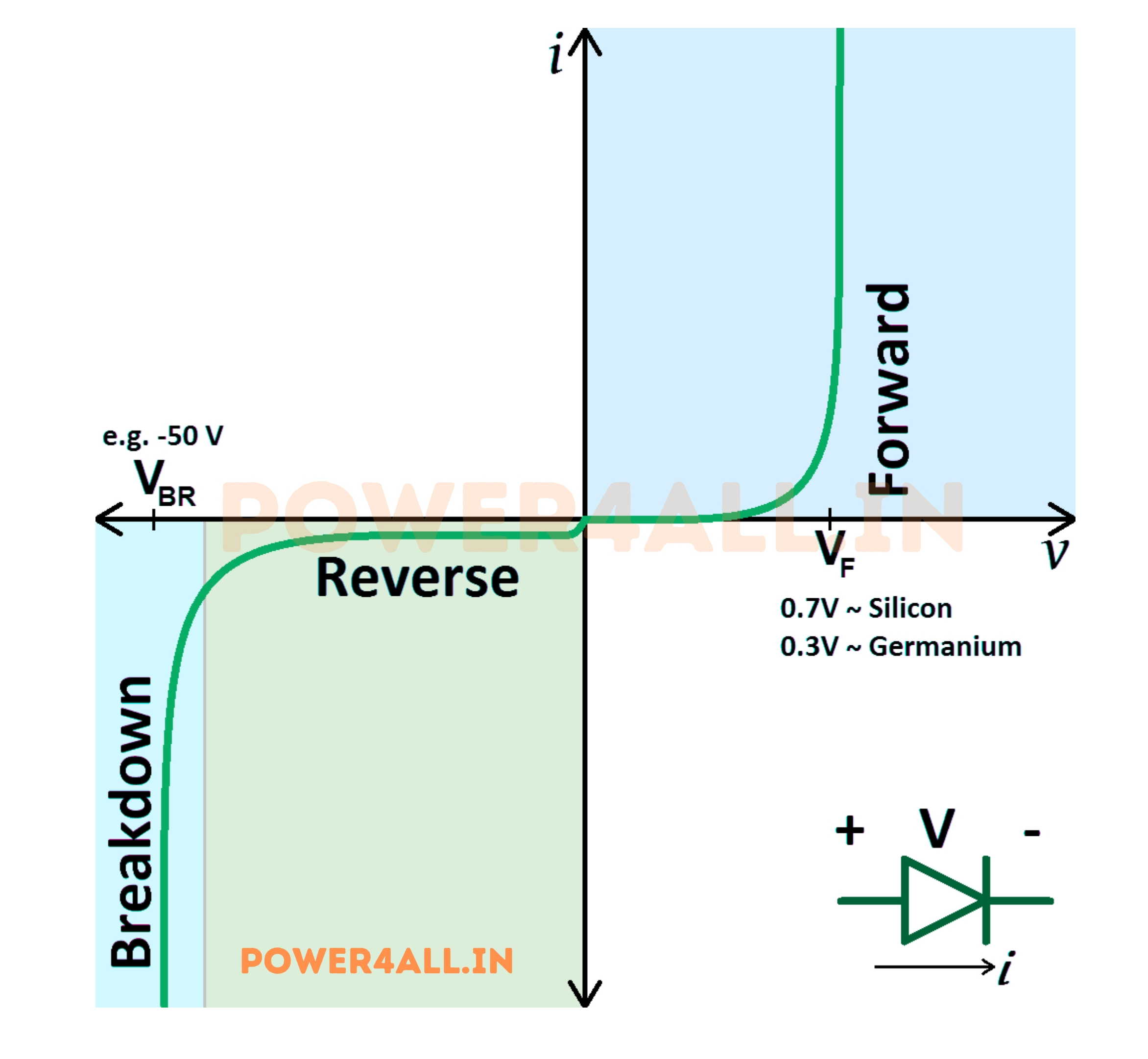
I-V Characteristics
Forward Bias Characteristics
The forward bias region shows exponential current increase with voltage. The curve starts flat near zero, then rises sharply after the knee voltage is reached.
Key Parameters
- Threshold voltage: 0.7V (Si), 0.3V (Ge), 0.2V (Schottky)
- Knee current: Current at onset of exponential region
- Series resistance: Limits current at high forward voltage
- Temperature coefficient: -2mV/°C for silicon diodes
I = IS(e^(V/nVT) - 1)
Shockley diode equation
Typical Forward Voltages
- Silicon rectifier: 0.6-0.8V at rated current
- Schottky diode: 0.2-0.4V at rated current
- LED (red): 1.8-2.2V at rated current
- LED (blue/white): 3.0-3.6V at rated current
Reverse Bias Characteristics
Reverse Leakage Current
Small but temperature-dependent current
Leakage Mechanisms
- Thermal generation: Minority carrier generation in depletion region
- Surface leakage: Current along crystal surface
- Junction tunneling: Quantum mechanical effect at high fields
- Parasitic resistances: Shunt resistance effects
Temperature Effects
- Leakage doubling: Every 10°C increase
- Exponential relationship: IR ∝ e^(T/T0)
- Material dependence: Silicon < Germanium < GaAs
- Surface effects: Humidity and contamination
Breakdown Characteristics
Maximum reverse voltage limits
Breakdown Types
- Avalanche breakdown: Impact ionization, >6V typical
- Zener breakdown: Field emission, <6V typical
- Thermal breakdown: Excessive power dissipation
- Surface breakdown: High electric field at edges
Breakdown Voltage Ratings
- PIV (Peak Inverse Voltage): Maximum repetitive reverse voltage
- PRV (Peak Reverse Voltage): Non-repetitive maximum
- Avalanche energy: Single pulse energy capability
- dV/dt rating: Maximum rate of voltage change
Dynamic Characteristics
| Parameter | Description | Typical Range | Impact on Circuits |
|---|---|---|---|
| Junction Capacitance | Voltage-dependent capacitance | 1pF - 1000pF | High-frequency response |
| Reverse Recovery Time | Turn-off switching time | 1ns - 100μs | Switching loss and EMI |
| Forward Recovery Time | Turn-on switching time | 1ns - 10ns | Rise time limitations |
| Thermal Time Constant | Thermal response time | 1ms - 10s | Thermal protection design |
Practical Operating Considerations
Temperature Derating
Current ratings must be derated with increasing temperature. Junction temperature is the limiting factor for power dissipation.
Surge Current Capability
Diodes can handle surge currents much higher than continuous ratings for short durations. I²t ratings specify surge capability.
Frequency Response
Junction capacitance and package inductance limit high-frequency performance. Schottky diodes offer best high-frequency response.
Reliability Factors
Proper voltage and current derating, thermal management, and protection from overcurrent ensure long diode life.
Operating Limits
Never exceed maximum ratings for voltage, current, or power. Use adequate safety margins and consider worst-case operating conditions including temperature, aging, and component tolerances.
Diodes vs Other Semiconductor Devices
Comparing diodes with transistors and other semiconductor devices helps understand when to use each component. While diodes are simple two-terminal devices, transistors offer amplification and switching with control terminals.
Diode vs Transistor Comparison
| Parameter | Diode | BJT | MOSFET | IGBT |
|---|---|---|---|---|
| Terminals | 2 (Anode, Cathode) | 3 (Base, Emitter, Collector) | 3 (Gate, Source, Drain) | 3 (Gate, Emitter, Collector) |
| Control Method | Voltage across device | Base current | Gate voltage | Gate voltage |
| Amplification | None | Yes (current gain) | Yes (voltage gain) | Yes (current gain) |
| Switching Capability | Passive (voltage dependent) | Active (controlled) | Active (controlled) | Active (controlled) |
| Power Handling | Very high (single function) | Medium | High | Very high |
| Switching Speed | Very fast (no control delay) | Medium | Very fast | Medium |
| Voltage Drop | 0.7V (fixed by physics) | VCE(sat) ≈ 0.2V | ID × RDS(on) | VCE(sat) ≈ 1.5V |
| Primary Applications | Rectification, protection | Amplification, switching | Switching, power control | High-power switching |
Application Selection Guidelines
When to Use Diodes
Simple, reliable one-way conduction
Ideal Applications
- Rectification: AC to DC conversion
- Freewheeling: Inductive load protection
- Voltage regulation: Zener diode regulators
- Reverse protection: Prevent reverse current
- Voltage references: Stable voltage sources
Advantages
- Simplicity: No control circuit needed
- Reliability: Fewer failure modes
- Cost: Lower cost than transistors
- High current: Excellent current handling
When to Use Transistors
Active control and amplification needed
Ideal Applications
- Switching control: Turn devices on/off remotely
- Amplification: Increase signal power
- PWM control: Precise power control
- Logic gates: Digital circuit building blocks
- Oscillators: Signal generation
Advantages
- Control: External signal control
- Amplification: Signal boost capability
- Efficiency: Low saturation voltage
- Integration: Multiple functions possible
Hybrid Solutions
Combining Diodes with Transistors for Optimal Performance
Complementary Circuit Design
Many circuits benefit from combining diodes and transistors, using each component where it performs best.
Protection Circuits
Transistor switching circuits often use diodes for flyback protection, ESD protection, and reverse polarity protection.
Power Supplies
Switching power supplies use transistors for switching and diodes for rectification and freewheeling functions.
Bias Circuits
Diode voltage drops provide stable bias voltages for transistor amplifiers, especially in temperature-compensated designs.
Common Hybrid Circuits
- H-bridge motor drivers: MOSFETs for switching, diodes for protection
- Buck converters: MOSFET switch, Schottky rectifier diode
- Class B amplifiers: Transistors for amplification, diodes for bias
- Voltage regulators: Pass transistor with Zener reference
Design Philosophy
Use the simplest device that meets requirements. Diodes for passive functions like rectification and protection, transistors when active control or amplification is needed. Consider cost, complexity, reliability, and performance in the selection process.
Diode Applications & Circuit Examples
Diodes are fundamental building blocks in countless electronic circuits. From simple rectification to complex protection schemes, understanding practical applications helps in designing effective and reliable electronic systems.
Power Supply Applications
Linear Power Supplies
Traditional transformer-based power conversion
Circuit Components
- Rectifier diodes: Convert AC to pulsating DC
- Filter capacitors: Smooth the rectified voltage
- Regulation: Zener diodes or linear regulators
- Protection: Fuses and surge protection
Design Considerations
- Diode voltage rating: 1.4× RMS input voltage minimum
- Current rating: 1.5-2× average load current
- Surge current: Capacitor charging current capability
- Heat dissipation: Forward voltage drop × current
Applications
- Laboratory supplies: Precision voltage regulation
- Audio equipment: Low-noise analog circuits
- Test equipment: Stable reference voltages
- Simple chargers: Battery charging circuits
Switching Power Supplies
High-efficiency power conversion
Diode Functions
- Output rectification: Fast recovery or Schottky diodes
- Freewheeling: Continuous current path
- Snubber circuits: Voltage spike suppression
- Input protection: Reverse polarity and surge
Performance Requirements
- Fast recovery: <100ns for high frequency
- Low forward drop: Schottky diodes for efficiency
- High temperature: 125-150°C junction rating
- Low EMI: Soft recovery characteristics
Topologies
- Buck converters: Step-down DC-DC conversion
- Boost converters: Step-up DC-DC conversion
- Flyback: Isolated power conversion
- Forward converters: Continuous energy transfer
Protection Circuit Applications
Overvoltage Protection
Protecting circuits from voltage spikes
Protection Methods
- TVS diodes: Fast transient suppression
- Zener clamps: Voltage limiting circuits
- Avalanche diodes: High-energy absorption
- Gas discharge tubes: Lightning protection
Application Examples
- ESD protection: USB, HDMI, Ethernet interfaces
- Automotive: Load dump and ignition transients
- Industrial: Motor drive and relay protection
- Telecom: Lightning and switching surges
Reverse Current Protection
Preventing damage from reverse current flow
Protection Scenarios
- Battery reverse connection: Polarity protection
- Solar panel blocking: Prevent reverse current at night
- Power supply backup: Prevent current from backup source
- Motor regeneration: Handle regenerative braking
Implementation Methods
- Series diode: Simple but with voltage drop
- Ideal diode controllers: MOSFET-based, no voltage drop
- Schottky diodes: Lower voltage drop solution
- Smart switches: Integrated protection and control
Signal Processing Applications
Diodes in Analog Signal Processing Circuits
Peak Detection and Clamping
Diodes enable peak detection, envelope detection, and voltage clamping in analog signal processing.
| Circuit Function | Diode Type | Key Feature | Applications |
|---|---|---|---|
| Peak Detector | Fast switching | Captures signal peaks | Audio level meters, RF power meters |
| Envelope Detector | Schottky | Follows signal envelope | AM demodulation, signal strength |
| Voltage Clamping | Zener or standard | Limits voltage excursion | Input protection, level shifting |
| Precision Rectification | Matched pairs | Full-wave rectification | AC measurement, RMS conversion |
RF and Communication Applications
RF Detection
Schottky and point-contact diodes detect RF signals in receivers, power meters, and antenna analyzers.
Frequency Mixing
Nonlinear diode characteristics enable frequency mixing for superheterodyne receivers and frequency converters.
Voltage Multipliers
Diode-capacitor networks create high voltages from low-voltage AC sources for CRT displays and ion generators.
Communication Circuit Examples
- Crystal radio: Diode detector for AM reception
- Mixer circuits: Frequency conversion in transceivers
- AGC circuits: Automatic gain control systems
- Phase detectors: PLL and frequency synthesis
Automotive and Industrial Applications
Automotive Electronics
Harsh environment applications
Engine Management
- Alternator rectification: High-current diode bridges
- Ignition protection: Flyback diodes on coils
- Sensor interfaces: Protection and level shifting
- Load dump protection: TVS diodes for transients
Body Electronics
- LED lighting: Headlights, taillights, indicators
- Motor protection: Window, seat, and mirror motors
- Relay drivers: Coil protection diodes
- Battery management: Charging and protection circuits
Industrial Control
Factory automation and process control
Motor Control
- VFD rectifiers: AC to DC conversion
- Freewheeling diodes: Continuous current paths
- Brake choppers: Regenerative energy dissipation
- DC bus protection: Overvoltage and fault protection
Sensors and Instrumentation
- Temperature sensors: Diode-based temperature measurement
- Photo sensors: Light detection and measurement
- Proximity detection: Infrared LED/photodiode pairs
- Safety systems: Light curtains and barriers
Application Design Tips
Select diodes based on specific application requirements: current rating, voltage rating, switching speed, and environmental conditions. Always include adequate safety margins and consider thermal management in high-power applications.
Rectifier Circuits and Power Conversion
Rectifier circuits convert alternating current (AC) to direct current (DC) using diodes. Understanding different rectifier topologies, their characteristics, and design considerations is essential for power supply design and AC-DC conversion applications.
Half-Wave Rectifiers
Basic Half-Wave Circuit
The simplest rectifier uses one diode to conduct current during only half of the AC cycle, resulting in pulsating DC output with significant ripple.
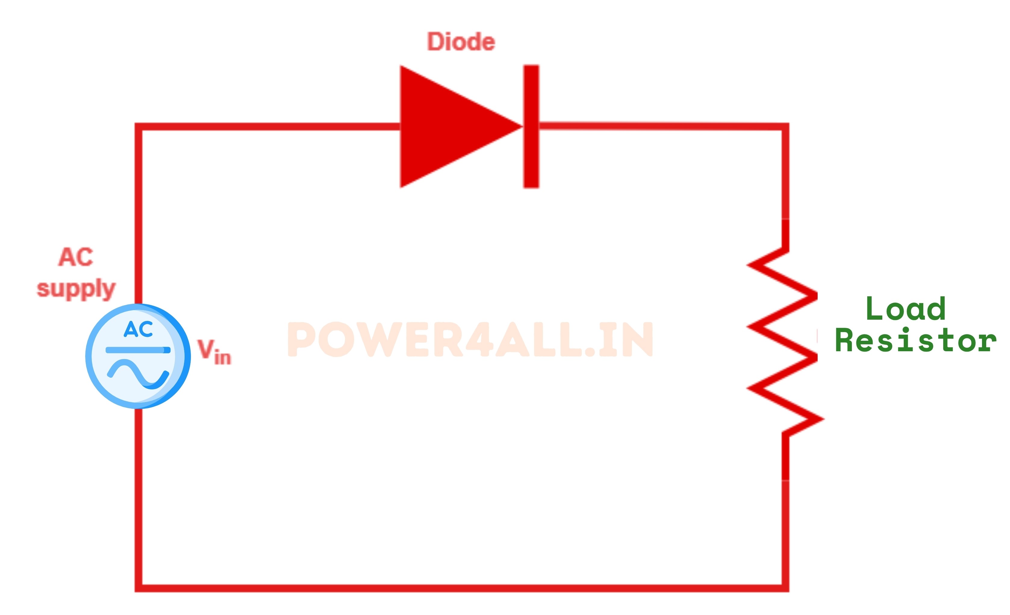
Circuit Operation
- Positive half-cycle: Diode conducts, current flows to load
- Negative half-cycle: Diode blocks, no current to load
- Output: Pulsating DC with 50% duty cycle
- Frequency: Output frequency = input frequency
VDC = VPeak / π ≈ 0.318 × VPeak
Average output voltage
Half-Wave Performance
- Efficiency: 40.6% maximum theoretical
- Ripple factor: 1.21 (high ripple content)
- PIV rating: Diode must withstand VPeak
- Transformer utilization: Poor (50%)
Full-Wave Rectifiers
Center-Tap Rectifier
Two diodes with center-tapped transformer
Circuit Configuration
- Transformer: Center-tapped secondary winding
- Diodes: Two diodes conducting alternately
- Load connection: Between center-tap and cathodes
- Current path: Always through one diode
Performance Characteristics
- Output voltage: VDC = 2VPeak/π ≈ 0.636 × VPeak
- Efficiency: 81.2% maximum theoretical
- Ripple frequency: 2× input frequency
- PIV rating: Each diode sees 2VPeak
Advantages and Disadvantages
- Pros: Good transformer utilization, low ripple
- Cons: Center-tapped transformer required, high PIV
- Applications: Low-voltage, high-current supplies
Bridge Rectifier
Four diodes in bridge configuration
Circuit Configuration
- Diode arrangement: Four diodes in diamond pattern
- Transformer: No center-tap required
- Conduction: Two diodes conduct per half-cycle
- Current flow: Bidirectional through transformer
Performance Characteristics
- Output voltage: VDC = 2VPeak/π (minus 2VF)
- Efficiency: Higher than center-tap (no center-tap loss)
- PIV rating: Each diode sees VPeak
- Transformer utilization: Excellent (better than center-tap)
Advantages
- No center-tap: Simpler transformer design
- Lower PIV: Half the voltage stress per diode
- Better efficiency: Improved transformer utilization
- Most popular: Standard for most applications
Filtering and Smoothing
Capacitor and Inductor Filters for Ripple Reduction
Capacitor Input Filters
Large electrolytic capacitors connected across the output smooth the pulsating DC by storing energy during peaks and supplying it during valleys.
| Parameter | Formula | Design Impact | Typical Values |
|---|---|---|---|
| Ripple Voltage | VR = IL/(f × C) | Larger C reduces ripple | 1-5% of DC output |
| Peak Current | IPeak = IL × π / (2 × θ) | High surge current through diodes | 5-10× average current |
| Conduction Angle | θ = π / (2 × RL × f × C) | Determines peak current | 30-60° typical |
| Filter Capacitor | C = IL/(f × VR) | Large capacitors for low ripple | 1000-10000μF typical |
LC and π Filters
L-C Filters
Inductor in series with load, capacitor in parallel. Provides excellent ripple reduction with continuous current through diodes.
π (Pi) Filters
Input capacitor, series inductor, output capacitor. Combines benefits of both C and LC filters with superior performance.
RC Filters
Series resistor with parallel capacitor. Simple and low-cost but with voltage drop across resistor.
Filter Design Guidelines
- Capacitor sizing: C = IL/(f × VR) for desired ripple
- Surge current: Use soft-start or NTC thermistors
- ESR effects: Low ESR capacitors for switching supplies
- Safety: Discharge resistors for high-voltage capacitors
Three-Phase Rectifiers
Three-Phase Half-Wave
Three diodes, one per phase
Circuit Characteristics
- Diodes: Three diodes with common cathode
- Conduction: Highest instantaneous phase voltage
- Ripple frequency: 3× line frequency
- Efficiency: Higher than single-phase
Performance
- Output voltage: 1.17 × VLine(RMS)
- Ripple factor: 0.17 (much lower than single-phase)
- Transformer utilization: Good
- Applications: Medium power DC supplies
Three-Phase Bridge
Six diodes for full-wave rectification
Circuit Configuration
- Diodes: Six diodes in three-phase bridge
- Conduction: Two diodes conduct simultaneously
- Line-to-line voltage: Utilizes full line voltage
- Ripple frequency: 6× line frequency
Advantages
- Highest efficiency: Best transformer utilization
- Lowest ripple: 6-pulse output
- No transformer center-tap: Simpler transformer
- High power: Suitable for kilowatt applications
Controlled Rectifiers
SCR and Thyristor-Based Variable DC Output
Phase-Controlled Rectifiers
Silicon Controlled Rectifiers (SCRs) replace diodes to provide variable DC output by controlling the firing angle.
Variable Output
Output voltage controlled by varying SCR firing angle. Later firing reduces average output voltage.
Motor Drives
DC motor speed control through variable DC voltage. Widely used in industrial applications.
Battery Chargers
Controlled charging current and voltage for different battery types and charge profiles.
Controlled Rectifier Applications
- DC motor drives: Variable speed control
- Electroplating: Controlled current density
- Battery charging: Multi-stage charging profiles
- Arc welding: Controlled welding current
Rectifier Design Guidelines
Select rectifier topology based on power level, efficiency requirements, and complexity constraints. Bridge rectifiers are most common for general use. Consider transformer utilization, diode stress, and filtering requirements in the design process.
Diode Selection & Design Guide
Selecting the right diode requires understanding application requirements and matching them with device characteristics. This comprehensive guide covers selection criteria, design calculations, and practical considerations for optimal diode choice.
Key Selection Parameters
| Parameter | Symbol | Importance | Design Impact | Selection Guidelines |
|---|---|---|---|---|
| Peak Inverse Voltage | PIV | Critical | Prevents breakdown | 2× maximum reverse voltage |
| Average Forward Current | IF(avg) | Critical | Thermal design | 1.5× application current |
| Forward Voltage Drop | VF | High | Power loss, efficiency | Minimize for efficiency |
| Reverse Recovery Time | trr | High | Switching losses | Fast diodes for switching |
| Junction Capacitance | Cj | Medium | High-frequency response | Low for RF applications |
| Surge Current Rating | IFSM | Medium | Inrush current handling | 10× steady-state current |
| Operating Temperature | TJ | High | Thermal management | Derate with temperature |
Application-Specific Selection
Power Supply Rectifiers
High current, efficient power conversion
Primary Requirements
- Current rating: Handle average and RMS currents
- Surge capability: Capacitor charging current
- Low forward drop: Minimize power loss
- Thermal management: Adequate heat sinking
Recommended Types
- Standard rectifiers: 1N540x series for general use
- Schottky diodes: Low voltage, high efficiency
- Fast recovery: Switching power supplies
- High current: Stud mount for >25A
Design Calculations
- Average current: IA = IL × duty cycle
- RMS current: IRMS = IA / √duty cycle
- Power dissipation: PD = VF × IA
- Heat sink: RθSA ≤ (TJ - TA)/PD - RθJC
Protection Applications
Protecting sensitive circuits from damage
ESD Protection
- TVS diodes: Fast response time <1ps
- Clamping voltage: Just above normal signal level
- Capacitance: Low for high-speed signals
- Bidirectional: For AC-coupled signals
Overvoltage Protection
- Breakdown voltage: 10-15% above normal voltage
- Power rating: Handle expected surge energy
- Response time: Fast enough for application
- Follow-on current: Circuit must limit current
Selection Guidelines
- Working voltage: 85% of breakdown voltage
- Peak power: 10ms pulse typically specified
- Package size: Thermal considerations
- Arrays: Multiple circuits in one package
Thermal Design Considerations
Heat Management and Thermal Calculations
Thermal Resistance Network
Diode thermal design involves understanding heat flow from junction to ambient through various thermal resistances.
Junction to Case
RθJC is the thermal resistance from junction to case/package. This is fixed by device construction and cannot be changed.
Case to Heat Sink
RθCS depends on thermal interface material and mounting method. Use thermal compound to minimize this resistance.
Heat Sink to Ambient
RθSA depends on heat sink size, surface area, airflow, and ambient conditions. This is the most controllable parameter.
Thermal Design Process
- Calculate power dissipation: PD = VF × IF
- Set maximum junction temperature: TJ ≤ 125°C (silicon)
- Determine ambient temperature: TA (worst case)
- Calculate required thermal resistance: RθJA = (TJ - TA)/PD
- Select heat sink: RθSA ≤ RθJA - RθJC - RθCS
TJ = TA + PD × (RθJC + RθCS + RθSA)
Junction temperature calculation
| Package Type | RθJC (°C/W) | RθCS (°C/W) | Mounting Notes |
|---|---|---|---|
| DO-35 (Glass) | 150-300 | N/A | PCB mounting, convection cooling |
| DO-41 (Plastic) | 50-100 | N/A | PCB mounting, larger thermal mass |
| TO-220 | 3-10 | 0.5-2 | Heat sink mounting, thermal compound |
| TO-247 | 0.5-2 | 0.2-1 | High power, large heat sink |
High-Frequency Considerations
RF and Microwave Diodes
High-frequency signal processing
Key Parameters
- Low capacitance: <1pF for GHz applications
- Fast switching: Recovery time <1ns
- Low noise: Minimize phase noise in oscillators
- Package parasitic: Minimize lead inductance
Recommended Types
- Schottky diodes: Zero recovery time
- Point contact: Ultra-low capacitance
- PIN diodes: RF switching applications
- Varactor diodes: Voltage-controlled oscillators
Switching Applications
Fast switching power electronics
Performance Requirements
- Fast recovery: <100ns for hard switching
- Soft recovery: Gradual current decay
- Low stored charge: Minimal reverse current
- Temperature stability: Consistent performance
Design Guidelines
- Snubber circuits: Reduce dV/dt stress
- Parallel connection: Current sharing for high power
- Thermal coupling: Matched thermal environments
- Gate drive optimization: Minimize switching losses
Cost and Reliability Optimization
Cost-Effective Design
Cost Reduction Strategies
- Use standard parts when possible
- Optimize for volume pricing
- Consider integrated solutions
- Balance performance vs. cost
- Plan for supply chain stability
Reliability Enhancement
- Adequate derating factors
- Quality supplier selection
- Environmental stress testing
- Redundancy in critical applications
- Preventive maintenance planning
Diode Testing & Troubleshooting
Effective diode testing and troubleshooting techniques are essential for circuit development and maintenance. Understanding how to test diodes with basic instruments and advanced equipment helps identify failures and optimize circuit performance.
Basic Diode Testing
Multimeter Testing
Simple go/no-go diode testing
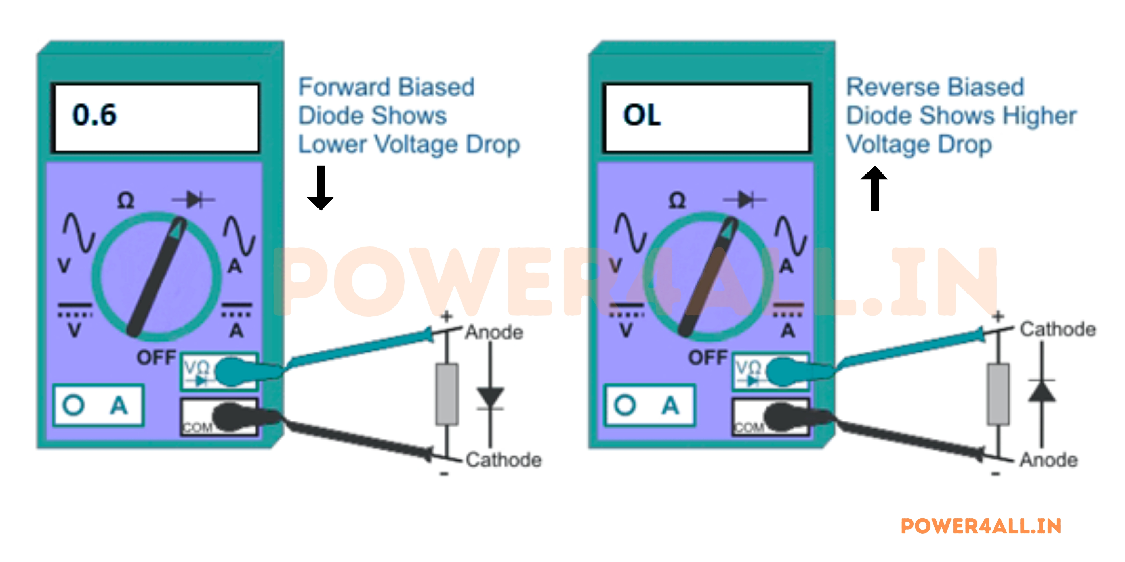
Diode Test Mode
- Forward test: Red probe to anode, black to cathode
- Expected reading: 0.6-0.8V for silicon, 0.2-0.4V Schottky
- Reverse test: Black probe to anode, red to cathode
- Expected reading: OL (overload) or very high resistance
Resistance Mode Testing
- Forward resistance: Low resistance (few hundred ohms)
- Reverse resistance: Very high resistance (MΩ range)
- Test voltage: Consider multimeter test voltage
- LED testing: May require higher voltage to see forward drop
Typical Test Results
- Good silicon diode: 0.7V forward, OL reverse
- Good Schottky: 0.3V forward, OL reverse
- Shorted diode: Low resistance both directions
- Open diode: OL reading both directions
In-Circuit Testing
Testing diodes without removal from circuit
Voltage Measurements
- Forward voltage: Should be ~0.7V when conducting
- Reverse voltage: Should be close to supply voltage
- Zero voltage: May indicate short circuit
- Full supply voltage: May indicate open circuit
Circuit Considerations
- Parallel paths: Other components may affect readings
- Bias conditions: Circuit may forward or reverse bias diode
- Power off testing: Remove power for resistance tests
- Isolation: May need to lift one lead for accurate test
Common Test Points
- Rectifier output: Check for AC ripple
- Protection circuits: Verify clamping action
- Freewheeling diodes: Check during switching
- Zener regulators: Verify regulation voltage
Advanced Testing Techniques
Curve Tracers and Parametric Testing
Curve Tracer Analysis
Curve tracers display complete I-V characteristics, allowing detailed analysis of diode behavior across full operating range.
| Test Parameter | Measurement Method | Information Gained | Failure Indicators |
|---|---|---|---|
| Forward Characteristics | I-V sweep, forward bias | Threshold voltage, series resistance | High voltage drop, soft knee |
| Reverse Leakage | I-V sweep, reverse bias | Leakage current vs. voltage | Excessive leakage, early breakdown |
| Breakdown Voltage | High voltage reverse sweep | Avalanche/Zener breakdown point | Low breakdown, soft breakdown |
| Dynamic Resistance | Slope of I-V curve | Small-signal resistance | High resistance, nonlinear |
Oscilloscope Testing
Switching Waveforms
Observe turn-on and turn-off behavior, measure recovery time, and identify ringing or overshoot problems.
Frequency Response
Test high-frequency performance using sine wave or pulse generators to characterize bandwidth limitations.
Reverse Recovery
Measure reverse recovery time and current using fast pulse generators and high-bandwidth oscilloscopes.
Oscilloscope Test Setup
- Probes: Use 10:1 probes to minimize loading
- Bandwidth: 5-10× signal frequency minimum
- Grounding: Short ground leads to minimize inductance
- Triggering: Use appropriate trigger levels and coupling
Common Failure Modes and Troubleshooting
Failure Mode Analysis
Understanding how and why diodes fail
Electrical Overstress
- Overvoltage: Exceeding PIV rating causes breakdown
- Overcurrent: Excessive current causes thermal damage
- dV/dt stress: Fast voltage changes can cause latch-up
- ESD damage: Static discharge destroys junction
Thermal Failures
- Overheating: Poor heat sinking or excess power
- Thermal cycling: Repeated temperature changes
- Wire bond failure: Thermal expansion mismatch
- Package degradation: Plastic package breakdown
Mechanical Failures
- Vibration damage: Wire bond or die attach failure
- Shock damage: Physical impact on package
- Humidity ingress: Corrosion and contamination
- Thermal shock: Rapid temperature changes
Troubleshooting Process
Systematic approach to problem solving
Problem Identification
- Symptom analysis: What is the observed problem?
- When did it start: Sudden or gradual failure?
- Operating conditions: Temperature, voltage, current
- Environmental factors: Humidity, vibration, contamination
Testing Strategy
- Visual inspection: Look for obvious damage
- Basic electrical tests: Multimeter measurements
- Comparative testing: Known good vs. suspect device
- Functional testing: In-circuit operation verification
Root Cause Analysis
- Circuit analysis: Check design for overstress
- Component history: Previous failures or issues
- Environmental factors: Operating conditions
- Quality issues: Manufacturing or handling problems
Troubleshooting Common Circuits
| Circuit Type | Common Problems | Symptoms | Troubleshooting Steps |
|---|---|---|---|
| Rectifier Circuits | No output, low output, high ripple | Dead circuit, reduced voltage, AC on output | Check diodes, filter capacitors, transformer |
| Voltage Regulators | No regulation, oscillation | Voltage varies with load, instability | Check Zener diode, feedback network, compensation |
| Protection Circuits | No protection, nuisance tripping | Damage during transients, false alarms | Verify trigger levels, check response time |
| LED Circuits | Dim light, no light, flickering | Reduced brightness, complete failure, instability | Check forward voltage, current limiting, thermal |
Testing Safety
Always observe proper safety procedures when testing diodes. Power off circuits before making resistance measurements. Use appropriate PPE when working with high-voltage circuits. Be aware that some circuits store energy in capacitors.
Diode Safety Considerations
Working safely with diodes requires understanding electrical hazards, proper handling procedures, and circuit safety considerations. Diodes can be found in high-voltage and high-current applications where safety is paramount.
Electrical Safety
High Voltage Precautions
Protection from dangerous voltages
Voltage Safety Guidelines
- Lockout/tagout: Ensure power cannot be restored
- Voltage verification: Test with calibrated meters
- Proper PPE: Insulated gloves, safety glasses
- Safe working distance: Maintain appropriate clearances
- Ground fault protection: GFCI where applicable
High-Voltage Applications
- CRT displays: Up to 30kV in picture tubes
- X-ray equipment: Hundreds of kV in medical devices
- Power transmission: HVDC converter stations
- Laser power supplies: High-voltage multipliers
High Voltage Warning
Diode circuits can operate at lethal voltages. Voltage multiplier circuits can generate many times the input voltage. Always assume circuits are energized until proven otherwise.
Energy Storage Hazards
Stored energy in capacitors and inductors
Capacitor Discharge
- Filter capacitors: Store significant energy in power supplies
- Discharge time: Can take minutes without bleeder resistors
- Discharge tools: Use insulated shorting sticks
- Verification: Measure voltage before touching circuits
Flyback Energy
- Inductive loads: Motors, relays, solenoids store energy
- Voltage spikes: Can be many times supply voltage
- Protection diodes: Freewheeling diodes prevent damage
- Snubber circuits: RC networks absorb energy
Energy Storage Examples
- TV power supply: 400V stored in main filter
- Camera flash: 300V in flash capacitor
- Motor drive: DC bus energy can be substantial
- Welding supply: High energy storage in filter capacitors
- UPS systems: Battery backup energy can be dangerous
Component Handling Safety
ESD Protection
Protecting sensitive diodes from static damage
ESD Sensitive Devices
- Schottky diodes: Metal-semiconductor junction sensitive
- LEDs: Especially blue and white high-brightness types
- Zener diodes: Low voltage types more sensitive
- RF diodes: Small geometry makes them vulnerable
ESD Prevention
- Grounded workspace: ESD mat and wrist strap
- Conductive packaging: Antistatic tubes and bags
- Humidity control: 40-60% relative humidity
- Ionized air: Neutralize static charges
ESD Voltage Levels
- Human body: Up to 25,000V static charge
- Diode damage: As low as 30-100V
- Detection threshold: 3,500V (human perception)
- Damage threshold: Often below perception level
Thermal Safety
Protection from heat-related hazards
Hot Surface Protection
- Heat sinks: Can reach burn-causing temperatures
- High-power diodes: Case temperatures >100°C possible
- Warning labels: Mark hot surfaces in accessible areas
- Guards and covers: Prevent accidental contact
Fire Prevention
- Proper rating: Never exceed diode specifications
- Heat sinking: Adequate thermal management
- Clearances: Keep combustibles away from hot parts
- Thermal protection: Fuses, breakers, thermal switches
Emergency Procedures
- Power disconnection: Know location of emergency stops
- Fire extinguishers: Class C for electrical fires
- First aid: Know burn treatment procedures
- Emergency contacts: Readily available phone numbers
Circuit Design Safety
Safe Design Practices and Protection Circuits
Protection Circuit Design
Incorporate multiple levels of protection to prevent diode failure and protect users from electrical hazards.
Overcurrent Protection
Use fuses, circuit breakers, or current-limiting circuits to prevent diode damage from excessive current.
Overvoltage Protection
Implement surge arresters, TVS diodes, or varistors to protect against voltage transients.
Thermal Protection
Include temperature monitoring and thermal shutdown to prevent overheating damage.
| Protection Type | Implementation | Response Time | Applications |
|---|---|---|---|
| Fast-acting Fuse | Series with diode | Microseconds | Semiconductor protection |
| TVS Diode | Parallel with protected circuit | Picoseconds | Transient suppression |
| Thermal Switch | Heat sink mounted | Seconds | Overtemperature protection |
| Current Sensor | Series current monitoring | Milliseconds | Electronic protection |
Safety Design Checklist
- Double insulation: Multiple barrier protection
- Fail-safe design: Safe failure modes
- Status indication: LEDs showing system state
- User isolation: No user access to hazardous voltages
- Emergency stops: Readily accessible shutoffs
Safety First
Always prioritize safety in diode circuit design and maintenance. Use appropriate personal protective equipment, follow lockout/tagout procedures, and ensure circuits are properly protected. When in doubt, consult qualified personnel and follow applicable safety codes and standards.
Frequently Asked Questions about Diodes
Common questions and comprehensive answers about diode operation, selection, applications, and troubleshooting to help engineers, students, and hobbyists understand and work effectively with diodes.
Basic Diode Questions
How does a diode work and why does it only conduct in one direction?
A diode works by forming a PN junction between P-type and N-type semiconductor materials. When the P-side (anode) is positive relative to the N-side (cathode), the built-in electric field is overcome, allowing current to flow. When reverse biased, the electric field is strengthened, blocking current flow except for tiny leakage currents.
The Physics Behind One-Way Conduction
- Forward bias: External voltage reduces the barrier, electrons flow from N to P side
- Reverse bias: External voltage increases the barrier, preventing current flow
- Depletion region: Acts like a voltage-controlled switch
- Threshold voltage: Minimum voltage needed to overcome the barrier (~0.7V for silicon)
Why do different diodes have different forward voltage drops?
Forward voltage drop depends on the semiconductor material and junction construction:
| Diode Type | Forward Voltage | Reason | Applications |
|---|---|---|---|
| Germanium | 0.3V | Lower bandgap energy | RF detection (historical) |
| Silicon | 0.7V | Standard bandgap | General purpose rectification |
| Schottky | 0.2-0.4V | Metal-semiconductor barrier | Low voltage, high efficiency |
| LED (Red) | 1.8-2.2V | Wide bandgap for red light | Indication, lighting |
| LED (Blue) | 3.0-3.6V | Very wide bandgap for blue light | White LED, displays |
How can I test if a diode is good or bad?
Simple Multimeter Test
- Set multimeter to diode test mode (usually has a diode symbol)
- Forward test: Red probe to anode, black to cathode - should read 0.6-0.8V
- Reverse test: Black to anode, red to cathode - should read "OL" (overload)
- Bad diode indicators: Reads same in both directions (shorted) or "OL" both ways (open)
Interpreting Test Results
- Good diode: 0.7V forward, OL reverse
- Shorted diode: Low reading both directions
- Open diode: OL reading both directions
- Leaky diode: Normal forward, low resistance reverse
Application Questions
When should I use a half-wave vs full-wave rectifier?
Half-Wave Rectifier
- Use when: Very simple, low-cost design needed
- Advantages: Only one diode needed, simple circuit
- Disadvantages: Poor efficiency (40%), high ripple, poor transformer utilization
- Applications: Simple LED circuits, basic DC supplies with light loads
Full-Wave Rectifier
- Use when: Better efficiency and performance needed
- Advantages: Higher efficiency (81%), lower ripple, better transformer utilization
- Disadvantages: More complex, requires more diodes
- Applications: Power supplies, motor drives, most practical DC conversion
Recommendation
Use full-wave rectifiers for virtually all applications except the simplest circuits. The improved performance and efficiency far outweigh the small increase in complexity and cost.
When should I use Schottky diodes instead of regular silicon diodes?
Choose Schottky Diodes When:
- Low voltage applications: 3.3V, 5V, 12V systems where 0.7V drop is significant
- High efficiency needed: Switching power supplies, battery-powered devices
- Fast switching required: High-frequency converters, RF applications
- Low forward drop critical: Output rectifiers in low-voltage supplies
Choose Silicon Diodes When:
- High voltage applications: >100V where forward drop is less significant
- High temperature operation: Schottky leakage increases rapidly with temperature
- Cost is primary concern: Silicon diodes are generally less expensive
- High current, low frequency: 60Hz rectification where switching speed doesn't matter
Practical Examples
- 5V power supply: Use Schottky for output rectifier (efficiency gain)
- 120V AC rectification: Use silicon rectifier diodes (cost effective)
- Automotive 12V: Use Schottky for efficiency, silicon for robustness
- Solar panel blocking: Use Schottky to minimize power loss
Design and Selection Questions
How do I select the right Zener diode for voltage regulation?
Zener Voltage Selection
- Regulation voltage: Choose Zener voltage equal to desired output
- Tolerance: ±5% typical, ±1% for precision applications
- Temperature coefficient: Choose based on temperature stability needs
- Voltage range: 2.4V to 200V commonly available
Power Rating Calculation
PZ = VZ × IZ(max)
Where IZ(max) = (VIN(max) - VZ) / RS
Design Steps
- Choose Zener voltage = desired output voltage
- Calculate maximum Zener current
- Select Zener power rating ≥ 2 × calculated power
- Calculate series resistor: RS = (VIN - VZ) / (IZ + IL)
- Verify regulation with load variations
Can I connect diodes in parallel to handle more current?
Yes, but diodes don't share current equally due to variations in forward voltage drop. Proper design techniques ensure reliable operation.
Current Sharing Issues
- Forward voltage variation: Even 50mV difference causes unequal sharing
- Temperature effects: Hottest diode carries more current (positive feedback)
- Manufacturing tolerance: VF variations between devices
- Thermal coupling: Different thermal environments affect sharing
Design Solutions
- Matched diodes: Select diodes with matched forward voltages
- Current sharing resistors: Small resistors (0.1-1Ω) in series with each diode
- Thermal coupling: Mount diodes on common heat sink
- Derating: Use 80% of combined current rating
Parallel Diode Design Example
Two 30A diodes in parallel for 50A load:
- Current sharing resistors: 5mΩ each (150mV drop at 30A)
- Power dissipation: 4.5W per resistor
- Thermal management: Common heat sink for both diodes
- Derating: Use 80% of 60A = 48A maximum
Troubleshooting Questions
Why is my LED dim or not lighting up properly?
Common LED Problems and Solutions
| Problem | Possible Causes | Solutions | Prevention |
|---|---|---|---|
| LED not lighting | Reverse polarity, blown LED, insufficient voltage | Check polarity, test LED, increase voltage | Mark polarity clearly, use protection |
| Dim light output | Low current, high temperature, aging | Increase current, improve cooling, replace LED | Proper current design, thermal management |
| Flickering | Loose connections, inadequate power supply, interference | Secure connections, improve supply, add filtering | Good mechanical design, proper bypassing |
| Color shift | Temperature effects, aging, overdrive | Control temperature, reduce current, replace | Thermal design, proper current limiting |
LED Troubleshooting Steps
- Check polarity with multimeter diode test
- Verify forward voltage matches LED specifications
- Measure current through LED with ammeter
- Check for proper heat sinking in high-power applications
- Test with known good LED to isolate problem
Mastering Diode Technology: Foundation of Modern Electronics
Diodes are the fundamental building blocks that enable the electronic world around us. From the simplest rectifier converting AC to DC power, to sophisticated LEDs providing efficient lighting, to protection circuits safeguarding expensive equipment, understanding diodes opens the door to mastering electronics design and troubleshooting.
Key Learning Outcomes
Fundamental Understanding
Diodes are voltage-controlled one-way valves formed by PN junctions, enabling current flow in only one direction when forward biased.
Diverse Applications
From rectification and voltage regulation to protection and light emission, diodes serve countless functions in modern electronics.
Design Expertise
Proper diode selection requires understanding application requirements, thermal management, and safety considerations.
The Diode Revolution
Impact on Technology
Diodes have revolutionized technology by enabling efficient power conversion, reliable circuit protection, energy-efficient lighting, and countless other applications that make modern life possible.
Historical Milestones
- 1906: First semiconductor diode (crystal detector)
- 1940s: Silicon PN junction diodes
- 1960s: LEDs enable solid-state lighting
- 1970s: Schottky diodes for efficiency
- 1990s: High-brightness LEDs
- 2000s: Wide bandgap semiconductors
Modern Applications
- Power electronics: Efficient AC-DC conversion in power supplies
- Renewable energy: Solar panel blocking and bypass diodes
- LED lighting: Energy-efficient illumination worldwide
- Circuit protection: ESD and surge protection in electronics
- Communication: Photodiodes in fiber optic systems
- Automotive: LED lighting and power management
Thank you for exploring the fundamental world of semiconductor diodes!
Continue your electronics education journey with our comprehensive guides on transistors, power electronics, and circuit design fundamentals.