Two-Switch Forward Converter
A forward converter with the primary sandwiched between two switches and two clamp diodes. The reset winding disappears, the leakage spike disappears, and every switch is held to just Vin instead of twice it.
- Introduction — fixing the forward converter’s weak spot
- What is a Two-Switch Forward Converter?
- Block Diagram
- Circuit Diagram & Construction
- Principle of Operation
- Modes of Operation
- Core Reset & the D ≤ 0.5 Limit
- Waveforms Explained in Detail
- Why the Switch Stress Halves
- Key Formulas
- Voltage Gain & Turns Ratio
- Worked Example
- Two-Switch vs Single-Switch Forward
- Advantages & Disadvantages
- Applications
- Frequently Asked Questions – FAQs
- Related Topics
Introduction — fixing the forward converter’s weak spot
The single-switch forward converter works beautifully, but it has one awkward feature: the reset winding. That third winding has to be wound bifilar with the primary, it pushes the switch voltage up to about twice the input, and it does nothing about the energy trapped in the transformer’s leakage inductance — which still spikes the switch at turn-off and still needs a dissipative snubber to survive.
The two-switch forward converter solves all of that with a neat trick: instead of adding a winding, add a second switch. Put the transformer primary between a high-side switch and a low-side switch, drive them both from the same gate signal, and add two clamp diodes across the pair. When the switches turn off, those diodes pin the winding directly to the supply rails. The core resets, the leakage energy is pushed back into the input rather than burned, and neither switch ever sees more than Vin.
This page builds that idea up: the parts, what happens in each half of the switching cycle, why the duty is still capped near 50 %, why the stress halves, the waveforms you would see on a scope, and a full worked example using exactly the same numbers as our single-switch forward page so you can compare them line by line.
What is a Two-Switch Forward Converter?
A two-switch forward converter is an isolated DC-DC converter — a forward converter in every respect that matters to the output, but with a different primary-side arrangement:
- Two switches, Q1 and Q2. Q2 sits between the positive rail and the top of the primary; Q1 sits between the bottom of the primary and ground. They are driven by one PWM signal and turn on and off together.
- Two clamp (catch) diodes, D1 and D2. D1 runs from ground to the top of the primary; D2 runs from the bottom of the primary up to the positive rail. They conduct only while the switches are off.
- An ordinary two-winding transformer — primary Np and secondary Ns, aiding dots, ungapped core. No reset winding.
- A secondary rectifier D3, a freewheel diode D4, and an L-C output filter — exactly the same output stage as any forward converter.
The whole innovation lives in that clamp pair. Because the primary is bracketed by two switches, when both open the winding has nowhere to go except into the two diodes — which tie its ends to ground and to Vin. That hard-clamps the winding at exactly −Vin, which both resets the core and holds each switch at Vin.
Block Diagram
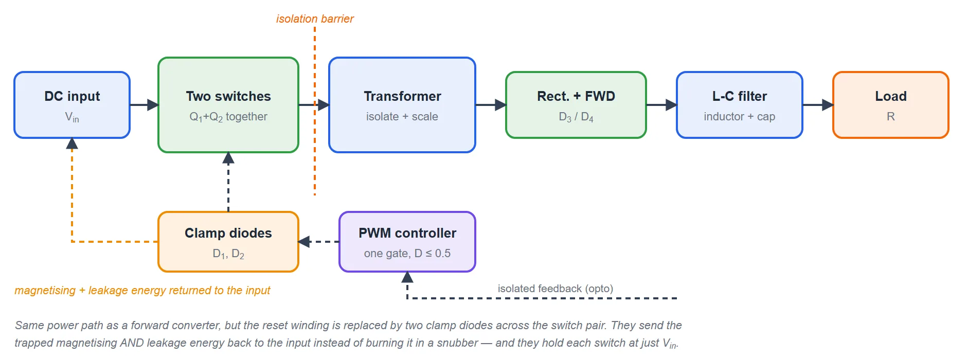
The power path is identical to a normal forward converter: input → switches → transformer → rectifier → L-C filter → load. What is new is the clamp block hanging off the switch pair, with its return arrow pointing back at the input. That arrow is the whole story: energy that a single-switch design would dump into a snubber resistor is instead given back to the supply. Note also that the controller drives one gate signal to both switches — there is no alternating or phase-shifted drive here.
Circuit Diagram & Construction
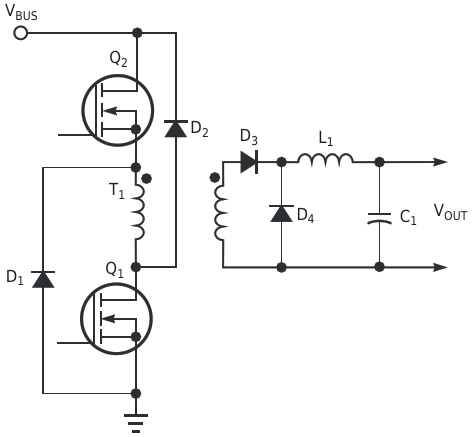
| Switch Q2 (high side) | Between the +Vin rail and node A (top of the primary). Its source floats, so it needs an isolated or bootstrapped gate drive — the one real cost of this topology. |
|---|---|
| Switch Q1 (low side) | Between node B (bottom of the primary) and ground. Ground-referenced, so simple to drive. Fires at the same instant as Q2. |
| Clamp diodes D1, D2 | The heart of the topology. When the switches open, D1 pulls node A down to ground and D2 pushes node B up to Vin. This clamps the winding at −Vin, resets the core, and returns both magnetising and leakage energy to the supply. |
| Transformer Np : Ns | An ordinary two-winding transformer with aiding dots and no air gap. No reset winding, so no fussy bifilar winding and lower leakage inductance. |
| D3 (rectifier), D4 (freewheel) | Standard forward output stage: D3 passes energy while the switches are on, D4 carries the inductor current while they are off. Each blocks about n·Vin. |
| Output filter L, C | Unchanged from the single-switch forward. The inductor keeps the load current smooth and continuous; its average is the load current. |
Principle of Operation
Both switches are driven by one signal, on for a fraction D of each period. So there are just two states, and the transformer sees a very simple, symmetric voltage:
- Both switches ON. The primary is connected straight across the supply: node A goes to Vin, node B goes to ground, so the winding sees +Vin. A scaled voltage n·Vin appears on the secondary, D3 conducts, and energy passes straight through to the L-C filter. Meanwhile the magnetising current ramps up.
- Both switches OFF. The magnetising current cannot stop, so it forces the clamp diodes into conduction. D1 ties node A to ground and D2 ties node B to Vin, so the winding now sees −Vin — the exact reverse. That drives the magnetising current back down to zero, resetting the core, while the current itself flows into the supply. On the secondary, D3 blocks and D4 freewheels the inductor current into the load.
Two consequences follow immediately, and they are the reasons this topology exists. First, since the reset voltage (−Vin) has the same magnitude as the on-voltage (+Vin), the reset takes exactly as long as the on-time — so the duty must stay at or below 0.5. Second, with node A clamped to 0 V and node B clamped to Vin, each switch is standing off exactly Vin and nothing more.
Modes of Operation
There are only two states per cycle. Follow each one on the power circuit in Figure 2 above.
Mode 1 — Both switches ON (powering)
- Q1 and Q2 close together, putting the full Vin across the primary (A at Vin, B at ground).
- The secondary produces n·Vin, forward-biasing D3. The inductor sees (n·Vin − Vo) and ramps up, delivering power to the load. D4 is reverse-biased.
- Both switches carry the same current — they are in series with the winding — equal to the reflected load current n·iL plus the magnetising ramp. The clamp diodes are reverse-biased and idle.
Mode 2 — Both switches OFF (clamp & reset)
- Both switches open. The magnetising current keeps flowing in the same direction through the winding, so it pulls node A down until D1 conducts and pushes node B up until D2 conducts.
- Now A is at 0 V and B is at Vin: the winding sees −Vin. The magnetising current ramps down at the same rate it ramped up, and it flows through D2 into the supply — the energy is recovered, not dissipated. The leakage energy takes the same path.
- Once the magnetising current reaches zero the clamps stop conducting, the winding voltage collapses to zero, and the two off switches simply share the rail (about Vin/2 each) for the rest of the period.
- On the secondary, D3 is reverse-biased and D4 takes over, freewheeling the inductor current into the load exactly as in any buck-derived converter.
Core Reset & the D ≤ 0.5 Limit
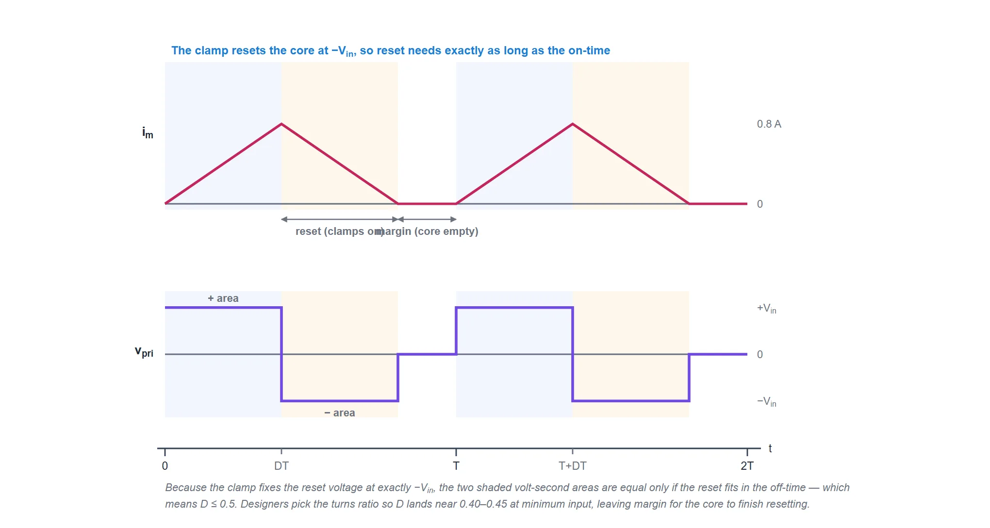
The reset mechanism here is simpler than the single-switch forward’s. There is no turns ratio to choose: the clamp diodes tie the winding straight to the rails, so the reset voltage is always exactly −Vin. Applying volt-second balance to the primary:
Vin · D·T = Vin · treset → treset = D·T | reset must fit: D·T ≤ (1−D)·T → D ≤ 0.5So the two-switch forward carries the same duty ceiling as a 1:1-reset single-switch forward — but it gets there without a reset winding, and the limit is now a fixed property of the circuit rather than something you trade against switch voltage. In practice designers pick the turns ratio so that at minimum input voltage the required duty lands around 0.40–0.45, leaving comfortable margin for the core to finish resetting before the next on-time.
Waveforms Explained in Detail
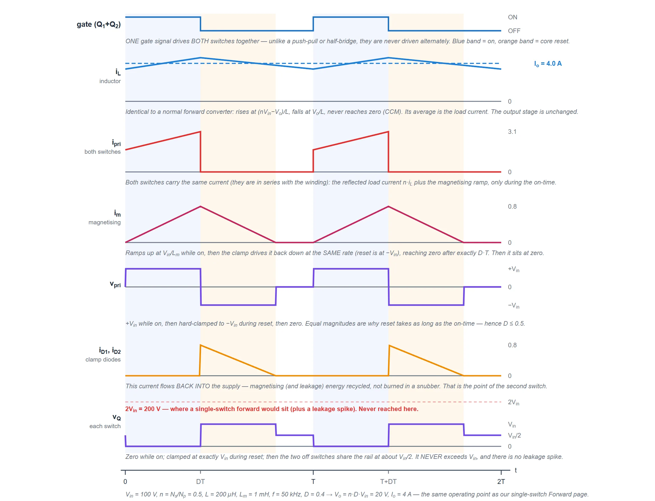
Read the traces together and the topology explains itself:
- Gate. A single signal driving both switches. On for DT, off for the rest. Note how different this is from a push-pull or half-bridge, where two gates alternate — here they fire as one.
- Inductor current iL. Completely unchanged from a normal forward converter: rises at (n·Vin−Vo)/L, falls at Vo/L, never touches zero, average equals the load current. The second switch changes the primary side, not the output.
- Primary current ipri. Both switches carry exactly the same current because they are in series with the winding: the reflected load current n·iL plus the small magnetising ramp, present only during the on-time.
- Magnetising current im. Ramps up at Vin/Lm, then the clamp drives it back down at the same slope, hitting zero after exactly D·T. It then sits at zero — the core is empty and waiting.
- Primary voltage vpri. A clean +Vin / −Vin / 0 sequence. The equal magnitudes are precisely why reset and on-time take equally long.
- Clamp-diode current. This one is worth staring at: it is current flowing backwards into the supply. That is the magnetising and leakage energy being recycled instead of burned in a snubber — the efficiency win that pays for the extra switch.
- Switch voltage vQ. Zero while on, a flat Vin = 100 V during reset, then about Vin/2 once the clamps release and the two off switches share the rail. The dashed line marks where a single-switch forward would have been sitting — at 200 V, plus a spike.
Why the Switch Stress Halves
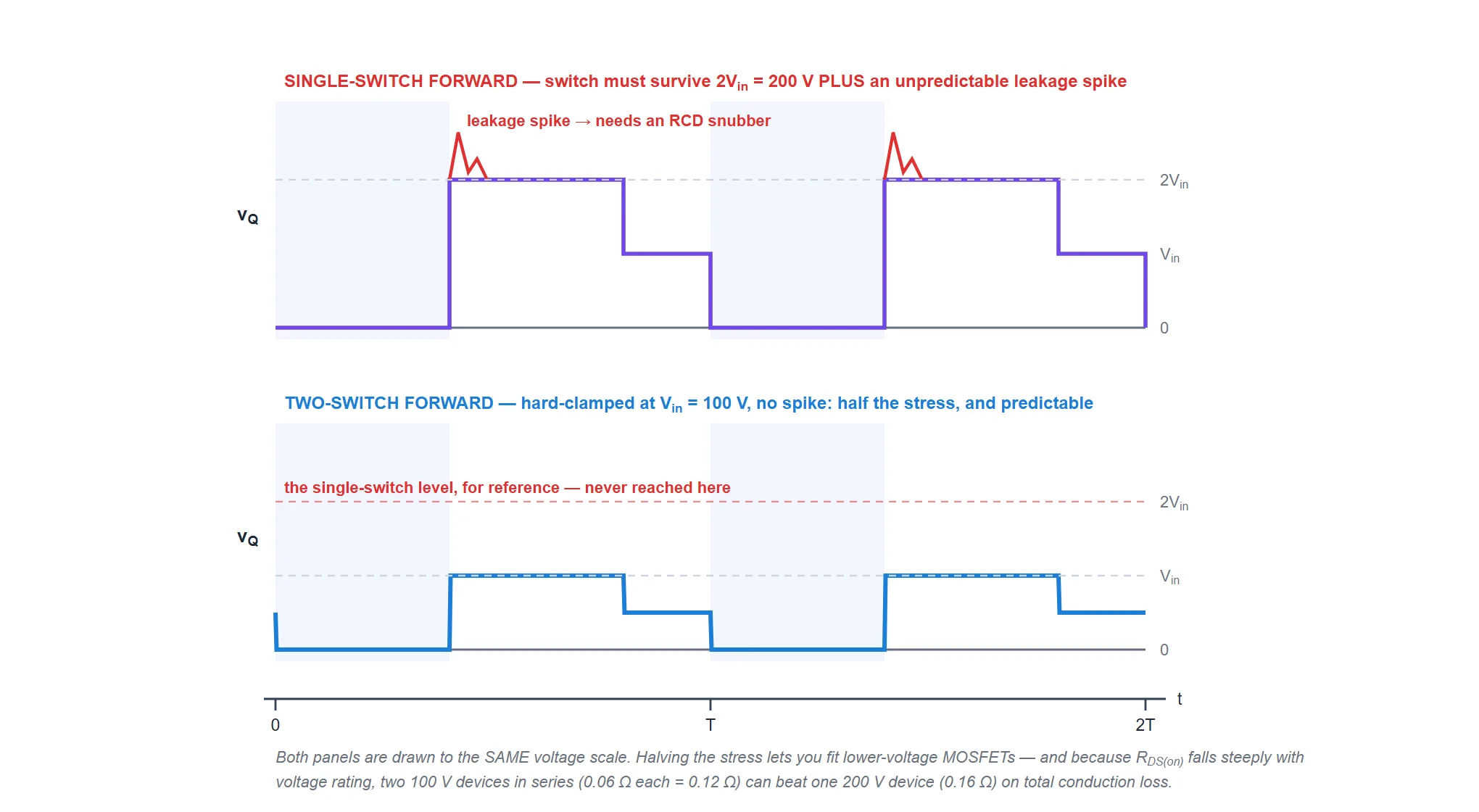
In a single-switch forward the off-state switch voltage is the input plus the voltage reflected back from the reset winding — with a 1:1 reset that is 2·Vin — and then the leakage inductance adds a ringing spike on top of that, whose height depends on how well the transformer happens to be wound. You must rate the MOSFET for the worst case, with margin.
In the two-switch version, node A physically cannot go below ground and node B physically cannot go above Vin, because diodes hold them there. The switch voltage is therefore hard-clamped at Vin, flat-topped, spike-free, and completely independent of leakage inductance. That has a very practical payoff:
The trade is honest, though: you pay with two gate drives (one of them high-side and floating), two extra components, and two sets of switching losses. On low-voltage inputs that rarely pays. On high-voltage buses — offline supplies running from a 400 V rail — it usually does.
Key Formulas
The output side is a buck, so everything follows from volt-second balance, with n = Ns/Np.
Output voltage (CCM) — identical to the single-switch forward:
(n·Vin − Vo)·D·T = Vo·(1−D)·T → Vo = n · D · VinDuty for a target output, and the reset limit:
D = Vo / (n · Vin) | treset = D·T | D ≤ 0.5 (design for 0.40–0.45 at Vin,min)Inductor ripple and average:
ΔiL = Vo·(1−D)·T / L | IL,avg = IoMagnetising current and device stress — note how simple the switch stress is:
Δim = Vin·D·T / Lm | VQ,off = Vin | VD1,D2 = Vin | VD3,D4 ≈ n·Vin(Ideal expressions; device drops and losses neglected. A practical two-switch forward runs around 88–93 % efficient, helped by the recovered leakage energy.)
Voltage Gain & Turns Ratio
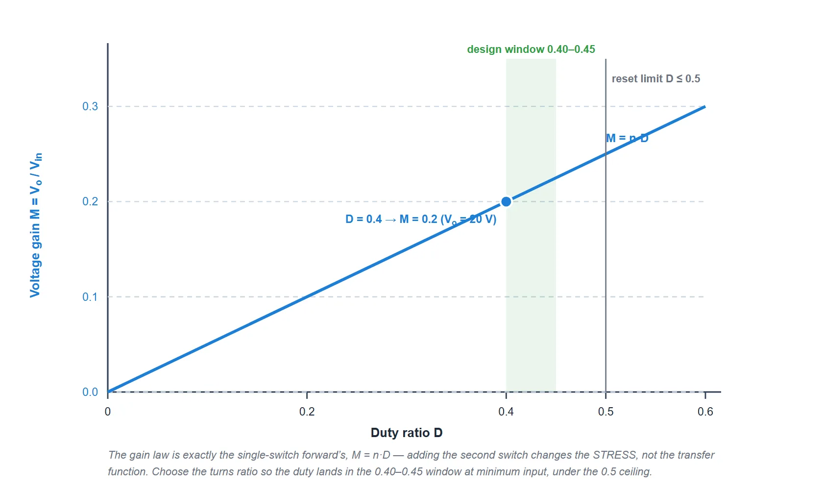
The gain law is exactly the single-switch forward’s straight line, M = n·D. This is worth emphasising: adding the second switch changes the stresses, not the transfer function. The converter is still a transformer-isolated step-down, still linear in duty, still easy to control.
- The turns ratio does the coarse scaling. Pick n so that the duty needed at minimum input lands in the 0.40–0.45 band; the duty then trims around it as the line and load move.
- The 0.5 ceiling is hard. Above it the core cannot finish resetting and will walk into saturation, so the maximum achievable output is n·Vin/2.
- Light load still means DCM. As in any buck-derived converter, if the inductor current reaches zero the output rises above n·D·Vin and becomes load-dependent, so L is sized to stay continuous over the working range.
Worked Example
Deliberately the same operating point as our single-switch forward example, so you can compare the two designs directly.
| Given | Vin = 100 V, Ns:Np = 1:2 (n = 0.5), D = 0.4, f = 50 kHz (T = 20 µs), L = 200 µH, Lm = 1 mH |
|---|---|
| Output voltage Vo = n·D·Vin | 0.5 × 0.4 × 100 = 20 V |
| Load (for Io = 4 A) R = Vo/Io, Po | R = 5 Ω, Po = 80 W |
| Inductor ripple ΔiL = Vo(1−D)T/L | 20 × 0.6 × 20µ/200µ = 1.2 A (Imax 4.6, Imin 3.4 → CCM) |
| Magnetising ramp Δim = Vin·D·T/Lm | 100 × 0.4 × 20µ/1m = 0.8 A |
| Reset time treset = D·T | 0.4 × 20µ = 8 µs < off-time 12 µs ✓ (4 µs margin) |
| Switch stress VQ,off = Vin | 100 V (single-switch forward: 200 V + leakage spike) |
| Clamp diodes VD1, VD2 | 100 V |
| Secondary diodes ≈ n·Vin | 0.5 × 100 = 50 V |
| Input current (avg) D·(n·Io) | 0.4 × 2 = 0.8 A → Pin = 100 × 0.8 = 80 W = Po ✓ |
Every output-side number is identical to the single-switch design — same 20 V, same 4 A, same 1.2 A ripple, same 8 µs reset. The only thing that changed is the switch stress: 100 V instead of 200 V plus a spike. That is the entire value proposition of the two-switch forward, and it is why it dominates offline designs where the bus voltage is high.
Two-Switch vs Single-Switch Forward
| Feature | Single-switch forward | Two-switch forward |
|---|---|---|
| Switches | 1 (ground-referenced) | 2, driven together (one is high-side) |
| Core reset | Reset (tertiary) winding + diode | Two clamp diodes to the rails |
| Reset voltage | −Vin·Np/Nt | Exactly −Vin |
| Switch stress | Vin(1+Np/Nt) ≈ 2Vin, plus leakage spike | Vin, hard-clamped, no spike |
| Leakage energy | Burned in an RCD snubber | Returned to the input |
| Snubber | Required | Not required |
| Transformer | 3 windings, bifilar primary/reset | 2 windings, simpler, lower leakage |
| Duty limit | D ≤ Np/(Np+Nt) | D ≤ 0.5 (fixed) |
| Gain | Vo = n·D·Vin — identical | |
| Gate drive | Simple, ground-referenced | Needs a floating/high-side drive |
| Best suited to | Low-voltage inputs, lowest cost | High-voltage buses (e.g. offline 400 V) |
Advantages & Disadvantages
Advantages
- Switch voltage clamped to Vin — roughly half a single-switch forward’s, and with no leakage spike on top. Predictable, so you can rate devices tightly.
- No dissipative snubber. Leakage energy is returned to the supply instead of being burned, improving efficiency and reducing heat.
- No reset winding. An ordinary two-winding transformer, easier and cheaper to wind, with lower leakage inductance to begin with.
- Lower-voltage MOSFETs become usable, and because RDS(on) scales steeply with rating, two of them in series can conduct better than one high-voltage part.
- Less ringing and lower EMI, because the clamped switching node has nothing to ring against.
- Simple gate-drive transformer is workable for the high-side device, since the duty is guaranteed below 50 %.
Disadvantages
- A high-side, floating gate drive is required for Q2 — the main added complexity.
- More components: an extra switch and an extra diode, plus the second drive circuit.
- Two devices in the conduction path, so two sets of switching losses and two forward drops — which is why the topology pays off mainly at higher bus voltages.
- Duty still capped at 0.5, so the input-voltage range and maximum gain are bounded just as in the single-switch forward.
- No zero-voltage switching by itself — it is still a hard-switched converter (the active-clamp forward addresses that).
Applications
- Offline (AC-DC) power supplies running from a rectified ~400 V bus, where clamping the switch to Vin lets you use 500 V MOSFETs instead of 800–1000 V parts — the classic use case.
- Telecom and datacom supplies from 48 V or high-voltage DC distribution buses.
- Industrial and server power modules in the roughly 100–500 W range where efficiency and reliability matter more than component count.
- Battery chargers and welding supplies with wide input ranges, where the predictable clamped stress simplifies device selection.
- Auxiliary and control supplies in high-voltage equipment such as drives, solar inverters and traction systems.
- Anywhere a single-switch forward is running out of voltage margin — the two-switch version is usually the first upgrade a designer reaches for.
The rule of thumb: the higher the input voltage, the more the two-switch forward is worth its extra parts. At low input voltages a plain forward or flyback is cheaper; at higher power a push-pull, half-bridge or full-bridge takes over.
Frequently Asked Questions – FAQs
Related Topics
- Forward Converter — the single-switch original
- Push-Pull Converter — two switches driving the core both ways
- Flyback Converter — the low-power isolated buck-boost
- Buck Converter (Step-Down) — the non-isolated parent
- DC-DC Converters — Overview
- MOSFET — the usual switch
- All Power Electronic Converters