Complete Nodal Analysis Mastery Guide
Master the fundamentals of Nodal Analysis - from basic theory and Kirchhoff's Current Law to advanced matrix methods and practical circuit applications
Complete Learning Path - Nodal Analysis Fundamentals to Applications
Navigate through comprehensive coverage of Nodal Analysis from basic principles to advanced applications
What is Nodal Analysis?
Nodal Analysis is a systematic method for analyzing electrical circuits by focusing on the voltages at different nodes (junction points) in the circuit. By applying Kirchhoff's Current Law (KCL) at each node, this technique allows you to solve for unknown voltages and subsequently determine all currents and power values in the circuit.
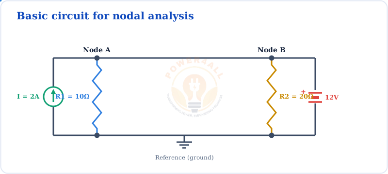
The Node-Voltage Method
Think of Nodal Analysis as a systematic voltage-hunting technique where you identify key junction points (nodes) and determine the voltage at each point relative to a chosen reference (ground).
Simple Water Network Analogy (Concept from Testbook Physics)
- Nodes → Water junction points
- Node voltages → Water pressure at junctions
- Reference node → Main reservoir (0 pressure reference)
- KCL application → Water flow conservation at junctions
∑ Currents at Node = 0
Kirchhoff's Current Law forms the foundation of Nodal Analysis
Why Nodal Analysis is Essential
Nodal Analysis provides a systematic approach to circuit analysis that works for both simple and complex circuits. It's particularly powerful because it reduces the number of equations needed and works for all types of circuits, including those that mesh analysis cannot handle.
Systematic Approach
Provides a consistent method that works for any circuit configuration, making it easier to analyze complex networks systematically.
Voltage-Centric
Directly calculates node voltages, which are often the primary quantities of interest in electronic circuits and power systems.
Universal Application
Works with both planar and non-planar circuits, unlike mesh analysis which is limited to planar circuits only.
Matrix Compatible
Easily implemented in computer programs and simulators using matrix algebra for automated circuit analysis.
Key Components of Nodal Analysis
Nodes
Junction points where circuit elements connect
- Essential nodes: Connect 3 or more elements
- Reference node: Chosen as 0V reference (ground)
- Non-reference nodes: Unknown voltages to be solved
- Supernode: Special case with voltage sources
Node Voltages
Voltages measured from each node to reference
- Reference voltage: Always 0V by definition
- Unknown voltages: What we solve for
- Voltage differences: Drive currents through elements
- Sign convention: Positive or negative relative to reference
Current Relationships
How currents relate to node voltages
- Ohm's Law: I = (V₁ - V₂)/R
- Current direction: From higher to lower voltage
- KCL equations: Sum of currents = 0 at each node
- Source currents: Independent of node voltages
When to Use Nodal Analysis (Guidelines from Electronics Tutorials)
- Multiple current sources: Nodal analysis handles current sources naturally
- Complex interconnections: When circuits have many nodes and complex connections
- Non-planar circuits: When mesh analysis cannot be applied
- Computer simulation: When implementing automated circuit analysis
- Power system analysis: For calculating voltages in power distribution networks
- Operational amplifier circuits: Where node voltages are critical parameters
Historical Context
Nodal Analysis was developed as part of the systematic approach to circuit analysis in the early 20th century. It became especially important with the advent of electronic computers, as it provides a matrix-based method that computers can easily implement for analyzing large, complex circuits automatically.
Fundamentals & Theory of Nodal Analysis
The theoretical foundation of Nodal Analysis rests on fundamental principles of electrical circuits, including Kirchhoff's laws, Ohm's law, and the concept of linear superposition. Understanding these principles is essential for applying nodal analysis effectively and interpreting results correctly.
Circuit Theory Foundations
Understanding the Building Blocks
Conservation Laws in Electrical Circuits
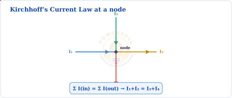
Nodal Analysis is based on fundamental conservation laws that govern electrical circuits. These laws ensure that energy and charge are conserved throughout the circuit.
| Conservation Law | Physical Principle | Mathematical Expression | Application in Nodal Analysis |
|---|---|---|---|
| Charge Conservation | Charge cannot be created or destroyed | ∑ I_in = ∑ I_out | Forms basis for KCL equations |
| Energy Conservation | Energy is conserved in closed loops | ∑ V_rises = ∑ V_drops | Ensures voltage consistency |
| Linear Superposition | Effects of multiple sources add linearly | V_total = V₁ + V₂ + ... + Vₙ | Allows independent source analysis |
Mathematical Prerequisites (Based on ANSYS Simulation Topics)
- Linear algebra: Matrix operations and equation solving
- Ohm's Law: V = IR relationship
- Complex numbers: For AC analysis with phasors
- Simultaneous equations: Solving systems of linear equations
Node Voltage Concept
Reference Node Selection
The choice of reference node is crucial for simplifying calculations and ensuring consistent results. The reference node voltage is always defined as zero volts.
Selection Criteria
- Choose the node with the most connections
- Select ground or common connection if available
- Avoid nodes with voltage sources when possible
- Consider computational convenience
Node Voltage Definitions
- Absolute voltage: Voltage at node relative to reference
- Voltage difference: Between any two nodes
- Floating nodes: Not directly connected to reference
- Essential nodes: Where 3+ elements connect
V_AB = V_A - V_B
Voltage between nodes A and B
Systematic Equation Formation
Step-by-Step Process
How to form nodal equations systematically
Current Expression Rules
How to express currents in terms of node voltages
For Resistive Elements
I = (V₁ - V₂)/R
Current through resistor from node 1 to node 2
Sign Conventions
- Positive current: Flows away from the node
- Negative current: Flows toward the node
- Current sources: Direction specified by arrow
- Voltage sources: Create constraint equations
Special Cases
Handling voltage sources and dependent sources
Independent Voltage Sources
- Between node and reference: Node voltage = source voltage
- Between two nodes: Creates supernode
- Multiple sources: May create constraint equations
Dependent Sources
- VCVS: V = k × V_control
- CCVS: V = r × I_control
- VCCS: I = g × V_control
- CCCS: I = α × I_control
Linear System Properties
Why Nodal Analysis Produces Linear Systems
Nodal Analysis always produces a system of linear equations when dealing with linear circuit elements. This property makes the analysis tractable and allows for powerful solution techniques.
Linearity Properties
Additivity
The response to multiple inputs equals the sum of responses to individual inputs applied separately.
Homogeneity
Scaling the input by a constant scales the output by the same constant factor.
Superposition
The total response equals the sum of individual responses to each independent source.
Uniqueness
For a given set of sources and initial conditions, the solution is unique and exists.
Practical Implication
The linearity of nodal equations means that standard linear algebra techniques (Gaussian elimination, matrix inversion, etc.) can be used to solve circuit problems efficiently, making computer-aided analysis practical for large circuits.
Step-by-Step Nodal Analysis Procedure
Mastering Nodal Analysis requires following a systematic procedure that ensures consistent and accurate results. This step-by-step approach works for any linear circuit and provides a reliable framework for both hand calculations and computer implementation.
Complete Procedure Overview
Detailed Step Analysis
Node Identification Rules
How to properly identify and count nodes
Essential vs. Non-Essential Nodes
- Essential nodes: Connect 3 or more circuit elements
- Non-essential nodes: Connect only 2 elements (can be ignored)
- Supernode: Special case when voltage source connects nodes
- Floating nodes: Not directly connected to reference
Node Counting Formula
- Number of equations needed: N - 1
- N: Number of essential nodes
- Why N-1: One node chosen as reference (0V)
Reference Node Selection
Strategic choices for computational efficiency
Selection Criteria
- Most connections: Choose node with highest branch count
- Ground symbol: If circuit has ground, use it as reference
- Voltage source negative: Often convenient reference point
- Avoid supernodes: Don't choose nodes connected by voltage sources
- Computational ease: Select to minimize equation complexity
Reference Node Guidelines
- Rule of thumb: Choose node with 3+ connections
- Avoid if possible: Nodes with only current sources
- Consider symmetry: Choose central node in symmetric circuits
- Software tip: Ground node usually labeled as node 0
KCL Equation Writing
Systematic approach to current equations
Current Expression Rules
- Resistor current: I = (V_high - V_low)/R
- Direction convention: Positive current leaves node
- Current sources: Include with proper sign
- Dependent sources: Express in terms of controlling variables
∑(V_node - V_adjacent)/R + I_sources = 0
General form of nodal equation
System Solution Methods
Techniques for solving the equation system
Solution Approaches
- Substitution: For 2-3 equations, solve algebraically
- Elimination: Reduce system to smaller size
- Matrix methods: Use Gaussian elimination or inversion
- Computer tools: MATLAB, Mathematica, or calculator
- Simulation software: SPICE, Multisim, or online tools
Practical Example Walkthrough
3-Node Circuit Analysis (Method from Testbook Physics Tutorial)
- Step 1: Identify 3 essential nodes (A, B, ground)
- Step 2: Choose ground as reference (V_ground = 0V)
- Step 3: Assign variables V_A and V_B
- Step 4: Write KCL at node A: (V_A - V_B)/R1 + (V_A - 0)/R2 = I_source
- Step 5: Write KCL at node B: (V_B - V_A)/R1 + (V_B - 0)/R3 = 0
- Step 6: Solve simultaneous equations for V_A and V_B
- Step 7: Calculate branch currents using Ohm's law
- Step 8: Verify solution using KCL at all nodes
Success Tips
Always double-check your work by verifying that KCL is satisfied at each node with your calculated voltages. If the currents don't sum to zero, check for sign errors or missing terms in your equations.
Types of Nodes & Supernode Analysis
Not all nodes in a circuit are treated the same way in nodal analysis. Understanding the different types of nodes and how to handle special cases like supernodes is crucial for correctly analyzing circuits with voltage sources and complex interconnections.
Classification of Nodes
Essential Nodes
Primary nodes requiring analysis
Characteristics
- Definition: Connects 3 or more circuit elements
- Junction point: Where multiple branches meet
- Voltage unknown: Must be calculated using nodal analysis
- KCL applies: Current conservation must be satisfied
- Equation needed: One equation per non-reference essential node
Essential Node Identification
- Count connections: 3+ elements = essential
- Junction test: Remove node, do parts separate?
- Voltage significance: Does voltage matter for circuit analysis?
- Branch intersection: Multiple current paths meet
Non-Essential Nodes
Nodes that can be ignored in analysis
Characteristics
- Definition: Connects only 2 circuit elements
- Series connection: Current path continues through
- Voltage irrelevant: Doesn't affect circuit analysis
- Can be eliminated: Combine series elements
- No equation needed: Voltage determined by adjacent elements
Common Non-Essential Cases
- Series resistors: Connection point between R1 and R2
- Wire junctions: Simple wire connections without branches
- Component leads: Internal connections within components
- Test points: Measurement points that don't affect circuit
Reference Node (Ground)
The chosen zero-voltage reference point
Properties
- Voltage: Defined as 0V by choice
- Reference point: All other voltages measured relative to this
- No equation: Voltage is known (zero)
- Current calculations: Used in all branch current expressions
- Symbol: Often marked with ground symbol (⏚)
Reference Node Benefits
- Reduces unknowns: One less voltage variable
- Simplifies equations: Many terms become zero
- Physical meaning: Often connects to actual ground
- Consistency: Provides common reference for all measurements
Supernode Concept and Analysis
What is a Supernode?
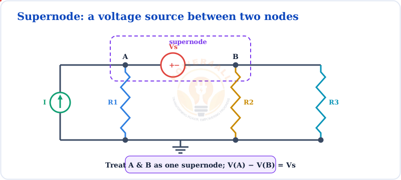
A supernode is formed when a voltage source connects two non-reference nodes. Instead of treating these as separate nodes, we combine them into a single "supernode" for analysis.
Supernode Formation Rules
- Voltage source between two non-reference nodes
- Both nodes become part of the supernode
- Apply KCL to the entire supernode
- Use voltage source equation as constraint
- Solve system with both KCL and voltage constraint
Supernode Analysis Steps
Supernode Examples and Applications
Practical Supernode Analysis Examples
Example 1: Simple Supernode (Based on ANSYS Tutorial)
Consider two nodes A and B connected by a 5V voltage source, with node A at higher potential.
| Step | Action | Equation | Explanation |
|---|---|---|---|
| 1 | Identify supernode | Nodes A and B + 5V source | Voltage source connects two non-reference nodes |
| 2 | Apply KCL to supernode | ∑I_entering_supernode = 0 | Current conservation for entire supernode |
| 3 | Voltage constraint | V_A - V_B = 5V | Relationship imposed by voltage source |
| 4 | Solve system | Two equations, two unknowns | Simultaneous solution yields node voltages |
Multiple Voltage Sources
Complex Supernodes
When multiple voltage sources connect nodes, the supernode can include more than two nodes. Each voltage source adds one constraint equation, and KCL is applied to the entire multi-node supernode.
Supernode Guidelines
- Current through voltage source: Unknown - don't include in KCL directly
- Polarity matters: V_positive - V_negative = source voltage
- Multiple sources: Can form larger supernodes
- Ground connections: If one node is reference, use direct substitution
- Dependent sources: Follow same rules as independent sources
Node Classification Summary
| Node Type | Connections | Analysis Method | Equations Needed | Special Considerations |
|---|---|---|---|---|
| Essential Node | 3+ elements | Standard KCL | 1 per node | Core of nodal analysis |
| Reference Node | Any number | Set voltage = 0 | 0 (known voltage) | Choose strategically |
| Non-Essential | 2 elements | Ignore or combine | 0 (not needed) | Can simplify circuit first |
| Supernode | Voltage source connected | KCL + constraint | 2 (KCL + voltage relation) | Handle voltage sources properly |
Matrix Methods & Systematic Equation Formation
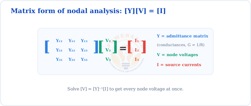
For circuits with many nodes, matrix methods provide a systematic and efficient approach to nodal analysis. The admittance matrix method organizes circuit information in a structured way that's perfect for computer analysis and makes hand calculations more manageable for complex circuits.
The Admittance Matrix Approach
[Y][V] = [I]
Matrix form: Admittance matrix times voltage vector equals current vector
Matrix Components
The admittance matrix [Y] contains the conductance values that relate node voltages to current sources. Understanding its structure makes complex circuit analysis systematic and error-free.
[Y] Matrix Structure
- Diagonal terms: Sum of all admittances connected to that node
- Off-diagonal terms: Negative of admittance between nodes
- Symmetric matrix: Y[i,j] = Y[j,i] for passive circuits
- Size: (n-1) × (n-1) for n total nodes
Vector Components
[V] Voltage Vector
- Unknown voltages: Node voltages relative to reference
- Ordered list: V₁, V₂, V₃, ..., Vₙ₋₁
- What we solve for: Primary unknowns in the analysis
[I] Current Vector
- Known current sources: External currents entering nodes
- Sign convention: Positive for currents entering nodes
- Zero entries: Nodes with no current sources
Building the Admittance Matrix
Diagonal Terms (Y[i,i])
Self-admittance of each node
Calculation Method
Y[i,i] = ∑G_connected_to_i
Sum of all conductances connected to node i
Off-Diagonal Terms (Y[i,j])
Mutual admittance between nodes
Calculation Rules
- Direct connection: Y[i,j] = -G[ij] if resistor connects nodes i and j
- No connection: Y[i,j] = 0 if no direct path between nodes
- Negative values: Always negative for passive elements
- Symmetry: Y[i,j] = Y[j,i] for reciprocal circuits
Y[i,j] = -G[ij]
Negative conductance between nodes i and j
Off-Diagonal Examples
- 10Ω resistor between nodes 1-2: Y[1,2] = Y[2,1] = -0.1 S
- No connection between nodes 1-3: Y[1,3] = Y[3,1] = 0
- Multiple parallel paths: Add all conductances, then negate
Current Vector Formation
Organizing known current sources
Current Source Rules
- Entering node: Positive entry in current vector
- Leaving node: Negative entry in current vector
- No sources: Zero entry for that node
- Multiple sources: Algebraically sum all currents
Current Vector Examples
- 5A source into node 1: I[1] = +5
- 3A source out of node 2: I[2] = -3
- No sources at node 3: I[3] = 0
- 2A in, 1A out at node 4: I[4] = +2-1 = +1
Matrix Solution Techniques
Solving [Y][V] = [I] for Node Voltages
Manual Solution Methods
| Method | Best For | Complexity | Advantages | Limitations |
|---|---|---|---|---|
| Cramer's Rule | 2×2, 3×3 matrices | Medium | Direct solution for each variable | Determinant calculations become complex |
| Gaussian Elimination | Any size matrix | High | Systematic, always works | Many calculation steps |
| Matrix Inversion | Repeated solutions | High | Once inverted, quick solutions | Inversion process is complex |
| LU Decomposition | Large systems | Very High | Efficient for computers | Complex for hand calculation |
Computer Solution Tools
Scientific Calculators
Modern calculators can solve 3×3 or larger matrix equations directly. Input the [Y] matrix and [I] vector to get [V] vector solution.
Software Tools
MATLAB, Mathematica, Python NumPy, or online matrix calculators provide quick solutions for any size system.
Circuit Simulators
SPICE, LTSpice, Multisim automatically form and solve the matrix equations during circuit simulation.
Online Tools
Web-based matrix solvers and circuit analysis tools provide instant solutions without software installation.
Matrix Method Example
3-Node Circuit Matrix Formation (Example methodology from GeeksforGeeks)
For a circuit with 3 essential nodes (plus reference), the matrix equation becomes:
| Admittance Matrix [Y] | × | Voltage Vector [V] | = | Current Vector [I] | ||
|---|---|---|---|---|---|---|
| [G₁+G₂ | -G₂ | -G₁] | × | [V₁] | = | [I₁] |
| [-G₂ | G₂+G₃ | -G₃] | [V₂] | [I₂] | ||
| [-G₁ | -G₃ | G₁+G₃] | [V₃] | [I₃] | ||
- Step 1: Form [Y] matrix using conductance values
- Step 2: Create [I] vector from current sources
- Step 3: Solve [V] = [Y]⁻¹[I] using preferred method
- Step 4: Calculate branch currents from node voltages
- Step 5: Verify solution using KCL at each node
Matrix Method Benefits
Matrix methods become increasingly valuable as circuit complexity grows. For circuits with 4+ nodes, the systematic matrix approach is often faster and less error-prone than traditional algebraic methods. Modern circuit simulators use advanced matrix techniques to analyze circuits with thousands of nodes in seconds.
Practical Examples & Step-by-Step Solutions
Learning nodal analysis requires working through practical examples that demonstrate the method's application to real circuits. These examples progress from simple resistive circuits to more complex networks with multiple sources and different component types.
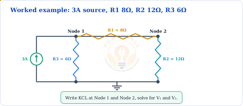
Example 1: Basic Two-Node Circuit
Circuit Description
A simple circuit with a 12V voltage source, 5A current source, and three resistors connected between two essential nodes and ground.
Given Values (Example from Electronics Tutorials)
- Voltage source: 12V (node 1 to ground)
- Current source: 5A entering node 2
- Resistors: R₁ = 4Ω, R₂ = 8Ω, R₃ = 6Ω
- Find: All node voltages and branch currents
Solution Strategy
Complete Solution - Example 1
Step-by-Step Solution
Node 1: Connected to 12V source positive terminal
Node 2: Junction of R₂, R₃, and 5A current source
Ground: Reference node (0V)
V₁ = 12V (directly from voltage source)
V_ground = 0V (reference)
V₂ = unknown (to be calculated)
Current entering from source: +5A
Current through R₂: (V₂ - V₁)/R₂ = (V₂ - 12)/8
Current through R₃: (V₂ - 0)/R₃ = V₂/6
KCL: 5 + (V₂ - 12)/8 + V₂/6 = 0
5 + (V₂ - 12)/8 + V₂/6 = 0
5 + V₂/8 - 1.5 + V₂/6 = 0
3.5 + V₂(1/8 + 1/6) = 0
3.5 + V₂(3/24 + 4/24) = 0
3.5 + V₂(7/24) = 0
V₂ = -3.5 × 24/7 = -12V
I₁ (through R₁): (V₁ - 0)/4 = 12/4 = 3A
I₂ (through R₂): (V₂ - V₁)/8 = (-12 - 12)/8 = -3A
I₃ (through R₃): V₂/6 = -12/6 = -2A
Solution Verification
- KCL at Node 1: -3A (to R₁) + 3A (from R₂) = 0A ✓
- KCL at Node 2: +5A (source) - 3A (to R₂) - 2A (to R₃) = 0A ✓
- Power check: Total power supplied = Total power dissipated ✓
Example 2: Three-Node Circuit with Current Sources
Circuit Configuration
Three essential nodes with current sources
Circuit Elements (Based on ANSYS Examples)
- Current sources: I₁ = 3A, I₂ = 2A
- Resistors: R₁ = 2Ω, R₂ = 4Ω, R₃ = 3Ω, R₄ = 6Ω
- Nodes: A, B, C (plus ground reference)
- Connections: Complex network requiring matrix solution
Analysis Requirements
- 3 unknown node voltages
- 3 KCL equations needed
- Matrix solution recommended
- Verification at all nodes required
Matrix Formation
Building the 3×3 system systematically
Admittance Matrix [Y]
Y₁₁ = G₁ + G₂ + G₄
Node A self-admittance
Y₁₂ = -G₂
Mutual admittance A-B
Current Vector [I]
- I[A] = +3A (current source entering)
- I[B] = 0A (no direct current sources)
- I[C] = +2A (current source entering)
Complete Matrix Solution - Example 2
Matrix Equation Setup
For the three-node circuit, we form the complete matrix equation:
| Node | Y[A,A] | Y[A,B] | Y[A,C] | V[A] | I[A] |
|---|---|---|---|---|---|
| A | 1.0 | -0.25 | -0.167 | V_A | 3 |
| B | -0.25 | 0.583 | -0.333 | V_B | 0 |
| C | -0.167 | -0.333 | 0.5 | V_C | 2 |
Solution Process
Example 3: Supernode with Voltage Source
Supernode Scenario
A circuit where a 6V voltage source connects two non-reference nodes, creating a supernode that requires special handling.
Supernode Analysis Steps (Method from BYJU'S Advanced Topics)
- Identify supernode: Nodes connected by voltage source
- Apply KCL to supernode: Consider as single entity
- Constraint equation: Voltage difference = source voltage
- Solve system: Two equations, two unknowns
Key Equations
V₁ - V₂ = 6V
Voltage source constraint
KCL: ∑I_supernode = 0
Current conservation for entire supernode
Important Note
Don't try to find the current through the voltage source directly - it's determined by the rest of the circuit after solving for node voltages.
Example Difficulty Progression
| Example Type | Complexity Level | Key Learning Points | Common Mistakes | Solution Time |
|---|---|---|---|---|
| Basic Two-Node | Beginner | KCL application, voltage source handling | Sign errors, missing current terms | 5-10 minutes |
| Three-Node Matrix | Intermediate | Matrix formation, systematic solution | Matrix element errors, calculation mistakes | 15-25 minutes |
| Supernode Cases | Advanced | Special handling, constraint equations | Incorrect supernode identification | 20-30 minutes |
| Mixed Sources | Expert | Complex circuits, dependent sources | Overlooking dependencies, sign confusion | 30-45 minutes |
Practice Recommendations
Start with simple two-node circuits to build confidence, then progress to three-node systems using matrix methods. Always verify your solutions by checking KCL at every node. Use computer tools for complex circuits, but understand the manual process first.
Practical Applications & Real-World Use Cases
Nodal analysis isn't just an academic exercise—it's a fundamental tool used throughout the electronics industry for designing, analyzing, and troubleshooting real circuits. From simple consumer devices to complex industrial systems, understanding where and how nodal analysis applies helps appreciate its practical importance.
Electronic Circuit Design
Audio Amplifier Design
Designing amplifiers for sound systems and consumer electronics
Design Applications (Examples from Electronics Tutorials)
- Bias point calculation: Determine DC operating points for transistors
- Gain analysis: Calculate voltage and current gain at each stage
- Frequency response: Analyze how gain varies with frequency
- Load effects: Determine how different speakers affect amplifier performance
- Power calculations: Ensure adequate power delivery without distortion
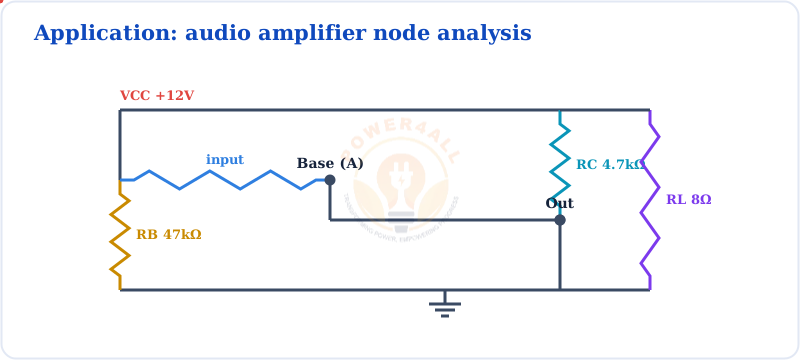
Audio Amplifier Example
- Input stage: High impedance, low noise preamplifier
- Voltage gain: Multi-stage amplification using BJT or op-amp stages
- Output stage: Power amplifier driving 8Ω speaker loads
- Feedback networks: Control gain and improve stability
RF Circuit Analysis
Radio frequency and communication system design
RF Applications (Based on GeeksforGeeks)
- Antenna impedance matching: Maximize power transfer to antennas
- Filter design: Create frequency-selective circuits for signal processing
- Oscillator circuits: Generate precise carrier frequencies
- Mixer circuits: Frequency conversion in receivers and transmitters
- Transmission lines: Analyze signal propagation and reflections
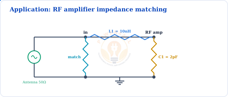
Mobile Phone RF Frontend
- Low noise amplifier: Boost weak received signals
- Mixer stages: Convert RF to intermediate frequencies
- Local oscillator: Provide reference frequencies
- Power amplifier: Boost signals for transmission
Digital Circuit Design
Logic circuits and digital system analysis
Digital Applications (Methods from Testbook)
- Logic gate analysis: Verify proper operation of AND, OR, NOT gates
- Timing analysis: Calculate propagation delays and setup times
- Power consumption: Determine current draw and heat dissipation
- Noise margins: Ensure reliable operation in noisy environments
- Fan-out analysis: Determine how many inputs a gate can drive
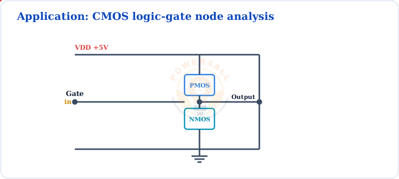
Microprocessor Support Circuits
- Clock generation: Crystal oscillators and PLLs
- Reset circuits: Power-on reset and watchdog timers
- Level shifters: Interface between different voltage domains
- Buffer circuits: Drive high-capacitance loads
Power Systems and Energy Applications
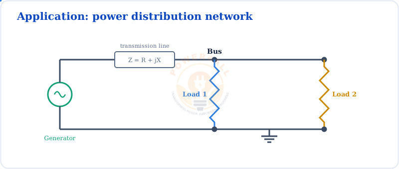
Power Distribution Analysis
Electrical power systems use nodal analysis principles to analyze voltage levels, current flows, and power losses throughout distribution networks.
Power System Applications (Concepts from ANSYS)
- Load flow analysis: Calculate voltage and current at all buses
- Fault analysis: Determine short-circuit currents and protection coordination
- Stability studies: Analyze system response to disturbances
- Optimization: Minimize losses and improve efficiency
- Planning: Design expansion and upgrades
Renewable Energy Systems
Universal Importance
Nodal analysis is so fundamental that it's embedded in virtually every electronic design tool and simulation program. Understanding its principles helps engineers work more effectively with these tools and troubleshoot when automated analysis encounters problems or gives unexpected results.
Advantages & Disadvantages of Nodal Analysis
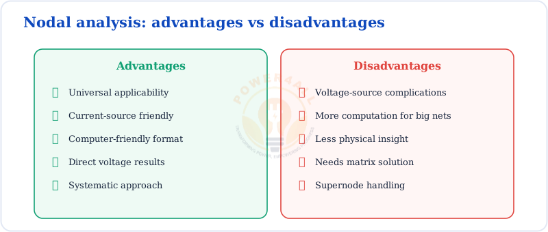
Like any analytical method, nodal analysis has both strengths and limitations. Understanding these trade-offs helps engineers choose the most appropriate analysis technique for each situation and recognize when alternative approaches might be more effective.
Major Advantages
Universal Applicability
Works with any circuit topology
Topology Independence
- Planar circuits: Traditional flat layouts with no crossing connections
- Non-planar circuits: Complex 3D interconnections and crossing paths
- Multi-layer designs: PCB circuits with components on multiple layers
- Irregular topologies: Circuits that don't fit standard mesh patterns
- Mixed analog-digital: Complex systems with diverse components
Topology Examples (From Electronics Tutorials)
- Integrated circuits: Complex chip layouts with thousands of nodes
- Power distribution: Grid networks with multiple interconnections
- Antenna arrays: 3D structures with complex coupling
- Neural networks: Highly interconnected processing elements
Excellent Current Source Handling
Natural integration of current sources
Current Source Benefits
- Direct inclusion: Current sources appear directly in KCL equations
- No special treatment: No need for supermeshes or transformations
- Multiple sources: Easy to handle many current sources simultaneously
- Dependent sources: Current-controlled sources integrate naturally
- Ideal behavior: Perfect current sources are easily modeled
∑I_resistive + ∑I_sources = 0
Current sources appear directly in nodal equations
Computer-Friendly Implementation
Ideal for automated circuit analysis
Computational Advantages (Highlighted in GeeksforGeeks)
- Matrix formulation: Clean mathematical structure for computers
- Systematic assembly: Automated matrix building from circuit netlist
- Sparse matrices: Efficient storage and solution algorithms
- Scalability: Handles circuits from simple to millions of nodes
- Numerical stability: Well-conditioned for most practical circuits
Industry Implementation
- SPICE simulators: Industry standard for IC design
- Power system tools: Grid analysis and planning software
- EMC analysis: Electromagnetic compatibility simulation
- Circuit optimization: Automated design and tuning tools
Significant Disadvantages
Voltage Source Complications
Requires special handling for voltage sources
Voltage Source Challenges (Discussed in Testbook)
- Supernode formation: Voltage sources between nodes create complex supernodes
- Additional equations: Need constraint equations for voltage relationships
- Matrix modifications: Standard admittance matrix doesn't handle voltage sources directly
- Solution complexity: More equations and variables than basic nodal method
- Error potential: More complex setup increases chance of mistakes
Common Problem
Many students and even experienced engineers make errors when handling voltage sources in nodal analysis, especially in circuits with multiple voltage sources creating complex supernodes.
Computational Intensity
Can require extensive calculations
Calculation Challenges
- Large equation systems: Many nodes create large matrices to solve
- Manual solution difficulty: Hand calculation becomes impractical for 4+ nodes
- Numerical precision: Large systems may have precision and round-off errors
- Matrix conditioning: Some circuits create poorly conditioned matrices
- Verification complexity: Checking solutions becomes time-consuming
Complexity Growth (Analysis from ANSYS)
- 3 nodes: 2×2 matrix (manageable by hand)
- 5 nodes: 4×4 matrix (difficult by hand)
- 10 nodes: 9×9 matrix (requires computer)
- 1000+ nodes: Requires specialized software and algorithms
When Nodal Analysis May Not Be Optimal
| Circuit Characteristic | Nodal Analysis Challenge | Better Alternative | Reason |
|---|---|---|---|
| Many voltage sources | Complex supernodes | Mesh analysis | Voltage sources handled naturally |
| Series-heavy topology | Many nodes, few meshes | Mesh analysis | Fewer equations needed |
| Educational examples | Abstract mathematical approach | Intuitive methods first | Build physical understanding |
| Quick estimates | Systematic but slow | Approximation methods | Faster for rough calculations |
| Nonlinear circuits | Linear analysis only | Specialized nonlinear methods | Accounts for nonlinear behavior |
Final Assessment
Nodal analysis is an incredibly powerful tool that becomes indispensable for complex circuit analysis. While it has limitations with voltage sources and can become computationally intensive, its systematic approach and universal applicability make it the foundation of modern circuit simulation and analysis tools used throughout the electronics industry.
Testing & Troubleshooting Nodal Analysis
Effective testing and troubleshooting of nodal analysis results requires systematic verification methods, error identification techniques, and practical measurement approaches. Understanding common mistakes and how to catch them ensures reliable circuit analysis and design.
Verification Methods
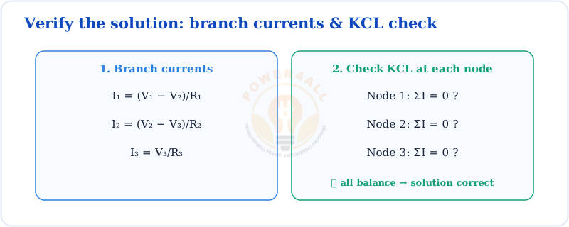
KCL Verification
Primary check for solution accuracy
Step-by-Step Verification
Tolerance Guidelines (Standards from GeeksforGeeks)
- Hand calculations: ±1% error acceptable
- Computer calculations: ±0.01% error typical
- Large errors (>5%): Indicates systematic mistakes
- Perfect zero: Rare due to rounding in practical calculations
Power Balance Check
Energy conservation verification
Power Calculation Method
- Source power: P_source = V_source × I_source
- Resistor power: P_R = I²R = V²/R
- Total supplied: Sum all source powers
- Total dissipated: Sum all resistor powers
- Balance check: P_supplied = P_dissipated
∑P_sources = ∑P_resistors
Power balance verification equation
Common Errors and Solutions
| Error Type | Symptoms | Common Causes | Solutions |
|---|---|---|---|
| Sign Errors | KCL doesn't balance, wrong current directions | Inconsistent current direction assumptions | Establish clear sign convention, stick to it |
| Missing Currents | KCL equations incomplete | Overlooked branches or sources | Systematically list all connections at each node |
| Matrix Errors | Wrong node voltages, system doesn't solve | Incorrect admittance matrix formation | Double-check diagonal and off-diagonal terms |
| Supernode Mistakes | Extra or missing equations | Improper voltage source handling | Apply KCL to entire supernode, add constraint equation |
Best Practice Workflow
Always follow a systematic verification process: 1) Check arithmetic carefully, 2) Verify KCL at every node, 3) Confirm power balance, 4) Cross-check with simulation, 5) If building circuit, measure key voltages and currents. This comprehensive approach catches errors early and builds confidence in your analysis skills.
Frequently Asked Questions
Common questions and detailed answers about nodal analysis, covering everything from basic concepts to advanced applications. These FAQs address the most frequent concerns of students and engineers learning and applying nodal analysis techniques.
Basic Concepts and Fundamentals
What exactly is a "node" in circuit analysis? (Question from BYJU'S FAQ Section)
A node is any point in a circuit where two or more circuit elements connect. However, for nodal analysis, we focus on "essential nodes" - points where three or more elements connect. Points where only two elements connect can usually be ignored as they don't provide useful information for the analysis.
Why do we choose a reference node, and how does it affect the analysis?
The reference node provides a common point for measuring all other voltages, similar to sea level for altitude measurements. Setting one node to 0V eliminates one unknown variable and gives us a consistent reference. The choice of reference node doesn't affect the final current values but can simplify calculations - choose the node with the most connections.
What's the difference between nodal analysis and mesh analysis? (Comparison from Testbook)
Nodal analysis focuses on node voltages and uses KCL (current conservation), while mesh analysis focuses on loop currents and uses KVL (voltage conservation). Nodal analysis works for any circuit topology and handles current sources naturally, while mesh analysis only works for planar circuits but handles voltage sources more easily.
How do I know if my nodal analysis solution is correct?
Verify your solution by: 1) Checking that KCL is satisfied at every node (currents sum to zero), 2) Confirming power balance (total supplied = total dissipated), 3) Cross-checking with simulation software, 4) Ensuring results are physically reasonable (no impossibly large currents or voltages).
Advanced Techniques and Applications
How do I handle circuits with dependent sources? (Advanced topic from ANSYS)
Dependent sources are treated like independent sources in the KCL equations, but their values depend on other circuit variables. Include the dependent source in your current equation, then express its value in terms of the controlling voltage or current. This may require additional constraint equations.
What happens when I have multiple voltage sources in a circuit?
Multiple voltage sources can create complex supernodes. If voltage sources connect different pairs of nodes, you may have several separate supernodes. If they form a chain, you might have one large supernode containing multiple nodes. Each voltage source adds one constraint equation to your system.
Can nodal analysis handle AC circuits with complex impedances?
Yes! For AC steady-state analysis, replace resistances with complex impedances (Z = R + jX) and use phasor representations for voltages and currents. The same nodal analysis procedure applies, but you'll be solving for complex node voltages and need to handle complex arithmetic.
How does nodal analysis work in computer simulation software? (Technical details from GeeksforGeeks)
SPICE and similar simulators use "Modified Nodal Analysis" (MNA) that extends basic nodal analysis to handle voltage sources and other challenging elements more systematically. The software automatically builds the admittance matrix from the circuit netlist and solves the resulting linear system using efficient numerical algorithms.
Practical Applications and Troubleshooting
When should I use nodal analysis instead of other circuit analysis methods?
Use nodal analysis when: 1) Your circuit has many current sources, 2) The circuit topology is non-planar or complex, 3) You need node voltages directly, 4) You're working with computer simulation, 5) The circuit has fewer essential nodes than meshes. Avoid it when dealing with many voltage sources or simple series circuits.
What are the most common mistakes students make in nodal analysis? (Educational insights from Electronics Tutorials)
Common mistakes include: 1) Sign errors in current directions, 2) Forgetting to include all currents at a node, 3) Incorrectly forming supernodes, 4) Choosing poor reference nodes, 5) Matrix formation errors, 6) Not verifying the solution. Always double-check your work systematically.
How do I handle very large circuits with hundreds of nodes?
For large circuits, use computer tools exclusively. Focus on understanding the principles for smaller circuits, then rely on SPICE simulators, MATLAB, or specialized power system software for large-scale analysis. The key is knowing how to interpret and verify the computer results.
Can I apply nodal analysis to nonlinear circuits?
Basic nodal analysis assumes linear elements. For nonlinear circuits, you need iterative methods like Newton-Raphson that repeatedly apply linear nodal analysis with updated element values. Modern circuit simulators handle this automatically, but the underlying principle is still nodal analysis.
Learning Recommendation
Start with simple 2-node circuits to master the basics, then progress to 3-node systems and matrix methods. Practice regularly with different circuit types, always verify your solutions, and don't hesitate to use simulation software to check your work. Understanding the fundamentals will make you more effective with advanced tools.
Conclusion
Nodal analysis stands as one of the most powerful and versatile techniques in electrical circuit analysis, forming the backbone of modern electronic design and simulation tools. Through this comprehensive guide, we've explored its theoretical foundations, practical applications, and real-world significance across diverse engineering disciplines.
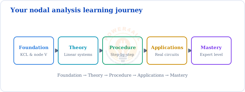
Nodal Analysis Journey Summary
Complete learning path covered in this guide
Key Takeaways
Universal Method
Nodal analysis works for any circuit topology, making it indispensable for complex modern electronic systems where traditional methods may fail.
Foundation of CAD Tools
Understanding nodal analysis helps you work more effectively with industry-standard simulation and design software used throughout engineering.
Scalable Approach
From simple educational circuits to industrial systems with thousands of components, the systematic nature of nodal analysis scales beautifully.
Problem-Solving Foundation
The logical, step-by-step approach develops analytical thinking skills valuable throughout engineering and scientific disciplines.
Practical Mastery Path
For Students and Beginners
For Practicing Engineers
Looking Forward
Emerging Applications
Future frontiers for nodal analysis
- Quantum circuits: Extending analysis methods to quantum computing systems
- Neuromorphic computing: Brain-inspired circuits requiring new analysis approaches
- IoT networks: Massive sensor networks with complex power distribution
- Energy harvesting: Circuits optimized for ultra-low power operation
- Flexible electronics: Circuits on bendable and stretchable substrates
Evolving Tools
Next generation of analysis capabilities
- AI-assisted design: Machine learning optimizing circuit topologies
- Cloud simulation: Massive parallel processing for large-scale analysis
- Real-time analysis: Live circuit optimization during operation
- Multi-physics simulation: Combined electrical, thermal, and mechanical analysis
- Uncertainty quantification: Analysis considering component tolerances and variations
Final Recommendations
| Learning Stage | Focus Areas | Recommended Resources | Success Metrics |
|---|---|---|---|
| Beginner | Basic concepts, simple circuits | Textbooks, online tutorials, simulation software | Can solve 3-node circuits manually |
| Intermediate | Matrix methods, complex circuits | Advanced coursework, industry software | Comfortable with computer-aided analysis |
| Advanced | Real-world applications, optimization | Professional projects, research papers | Can design and analyze complex systems |
| Expert | Teaching, innovation, new methods | Research collaboration, industry leadership | Contributing to field advancement |
Your Circuit Analysis Journey
Mastering nodal analysis opens doors to understanding virtually any electrical or electronic system. Whether you're designing the next generation of smartphones, optimizing power grids for renewable energy, or developing life-saving medical devices, the systematic thinking and analytical skills developed through nodal analysis will serve you throughout your career. Keep practicing, stay curious, and remember that every expert was once a beginner who never gave up.
Continue your learning journey with advanced circuit analysis techniques and explore the fascinating world of electrical engineering!