Active-Clamp Forward Converter
A forward converter that resets its core with an active clamp instead of a lossy snubber or reset winding — recycling the magnetising energy, soft-switching the transistors (ZVS), and freeing the duty cycle from the usual 50 % limit.
- Introduction — the forward converter’s reset problem
- What is an Active-Clamp Forward Converter?
- Block Diagram
- Circuit Diagram & Construction
- Principle of Operation
- Modes of Operation
- Zero-Voltage Switching Explained
- Waveforms Explained in Detail
- Switch Stress & the Duty-Cycle Freedom
- Key Formulas
- Voltage Gain & Turns Ratio
- Worked Example
- Active-Clamp vs Plain & Two-Switch Forward
- Advantages & Disadvantages
- Applications
- Frequently Asked Questions – FAQs
- Related Topics
Introduction — the forward converter’s reset problem
Every forward converter has to solve one awkward problem: once the switch turns off, the energy stored in the transformer’s magnetising inductance has to go somewhere, and the core has to be reset (its flux driven back to the start) before the next cycle — otherwise the flux “walks” and the transformer saturates. The classic answers are a reset (tertiary) winding, which pushes the switch voltage up towards twice the input, or an RCD snubber, which simply burns the energy in a resistor. Both waste power and both limit the usable duty cycle.
The active-clamp forward converter replaces that passive reset with an active one. A small reset capacitor Ccl in series with an auxiliary MOSFET M2 is placed across the primary. While the main switch is off, the auxiliary switch turns on and lets the capacitor resonate with the magnetising inductance: the core is reset gently, the magnetising energy is stored and returned rather than dissipated, and — the real prize — that same stored energy is used to swing the main switch’s drain to zero volts just before it turns on. The converter soft-switches.
This page builds the idea up from the parts: what each component does, the four things that happen in one switching cycle (including the two dead-times where the zero-voltage switching actually occurs), why the duty is now free to run past 50 %, the price you pay in switch voltage, the waveforms you would see on a scope, and a full worked example using the same numbers as our other isolated-converter pages so you can compare them directly.
What is an Active-Clamp Forward Converter?
An active-clamp forward converter is an isolated DC-DC converter — a forward converter in its power path — in which the core-reset job is done by an actively switched clamp circuit:
- Main switch M1. The ordinary forward switch, between the switching node and ground, driven by a PWM signal for a fraction D of each period.
- Active clamp: Ccl + M2. A reset capacitor in series with an auxiliary MOSFET, connected across the primary. M2 is driven out of phase with M1 — it is on precisely when M1 is off.
- Magnetising inductance Lm of the transformer — the element that stores the energy the clamp has to manage, and that resonates with Ccl during reset.
- Lump capacitances Cx1, Cx2 — the collected output capacitances of the devices at each switching node. Normally a nuisance; here they are part of the ZVS resonance.
- A standard forward output stage — rectifier diode D1, freewheel diode D2, output inductor Lo, capacitor Co and load Ro.
Block Diagram
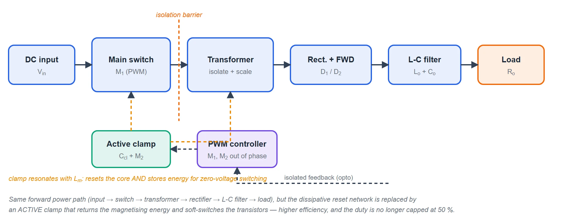
The main signal path is a normal forward converter: input → switch → transformer → rectifier → L-C filter → load. What is different is the active-clamp block hanging across the primary. Instead of a snubber resistor that turns trapped energy into heat, the clamp resonates that energy with the magnetising inductance and hands it back — and in doing so it sets up the zero-voltage switching. The controller drives two complementary gate signals (M1 and M2 out of phase), with a short dead-time between them where the soft transitions happen.
Circuit Diagram & Construction
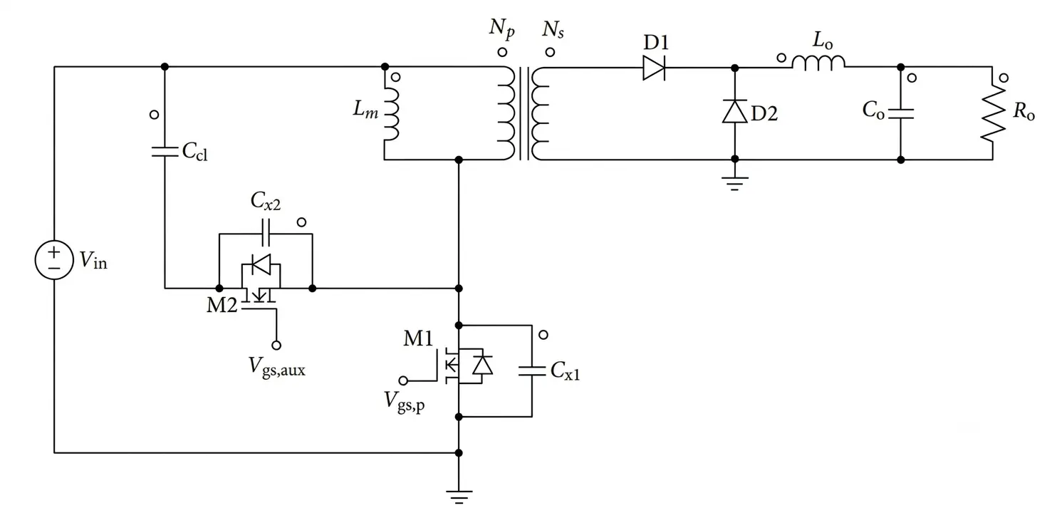
| Main switch M1 | The forward switch, from the switching node (bottom of the primary) to ground. Ground-referenced, driven by the main PWM signal Vgs,p for a fraction D of each period. |
|---|---|
| Lump capacitor Cx1 | The combined output capacitance seen at the switching node (M1, the secondary diodes reflected back, and the winding capacitance). It is charged and discharged resonantly during the dead-times — this is the capacitance ZVS drives to zero. |
| Active clamp Ccl + M2 | The heart of the topology. The reset capacitor Ccl in series with the auxiliary MOSFET M2, connected in parallel with the primary. When M1 is off, M2 is on, and Ccl resonates with Lm to reset the core and store the magnetising energy. Cx2 is M2’s own output capacitance. |
| Magnetising inductance Lm | Shown explicitly across the primary. In this converter it is a working element: its (bipolar) current carries the reset action and provides the energy that achieves zero-voltage switching. |
| Transformer Np : Ns | An ordinary two-winding transformer with aiding dots (forward action) and an ungapped core. No reset (tertiary) winding is needed — the clamp does that job. |
| D1 (rectifier), D2 (freewheel) | The standard forward output pair: D1 passes energy to the filter while M1 is on, D2 carries the inductor current while M1 is off. (In high-current designs both are often replaced by synchronous MOSFETs.) |
| Output filter Lo, Co | Exactly the forward output filter. The inductor keeps the load current smooth and continuous; its average is the load current. |
Principle of Operation
The two switches are driven out of phase: when the main switch M1 is on, the auxiliary switch M2 is off, and vice-versa, with a short dead-time between them where both are off. Over one period the transformer therefore sees a simple, self-balancing sequence:
- M1 on (on-time). The primary is connected across the input, so it sees roughly +Vin. A scaled voltage n·Vin appears on the secondary, the rectifier D1 conducts, and energy passes straight through to the L-C filter — ordinary forward action. The magnetising current ramps up.
- M2 on (off-time). The main switch is off and the clamp is connected. The reset capacitor Ccl now sits across the primary through M2, applying a reverse voltage −Vcl that drives the magnetising current back down — and past zero, negative. The core is reset over the entire off-time, and the energy goes into Ccl rather than into a resistor.
- Dead-times. In the brief gaps where both switches are off, the magnetising / clamp current charges and discharges the lump capacitances (Cx1, Cx2). This is where the switching nodes swing softly from one rail to the other so that the next switch to turn on does so at zero volts.
Two consequences make this converter special. First, because the reset voltage Vcl adjusts itself (it is whatever value balances the volt-seconds on the core), the reset always fits inside the off-time no matter what the duty is — so the 50 % ceiling of a plain or two-switch forward is gone. Second, the reset current is deliberately allowed to reverse, and that reversed current is exactly what is needed to achieve zero-voltage switching.
Modes of Operation
There are four intervals in each switching cycle: the two long ones where a switch conducts, and the two short dead-times where the soft transitions happen. Follow each one on the power circuit in Figure 2 above — the same single circuit explains all four, so no separate mode schematics are needed.
Mode 1 — On-time: power transfer (M1 on, M2 off)
- M1 is closed, so the switching node is pulled to ground and the full input voltage appears across the primary (top of the winding at Vin, bottom at 0). The clamp branch is idle because M2 is open.
- On the secondary the aiding dots give a positive voltage n·Vin, forward-biasing the rectifier D1. The output inductor sees (n·Vin − Vo) and ramps up, delivering power to the load; the freewheel diode D2 is reverse-biased.
- The main switch carries the reflected load current n·iLo plus the rising magnetising current. The magnetising current climbs from its negative starting value up through zero to its positive peak.
Mode 2 — First dead-time: soft turn-on of M2
- M1 turns off. The magnetising current (now at its positive peak) has nowhere to go through M1, so it flows into the lump capacitance Cx1, charging the switching node up from 0 toward Vin + Vcl.
- When the node reaches that clamp level, the body diode of the auxiliary switch M2 becomes forward-biased and begins to conduct the current. The voltage across M2 is now essentially zero.
- M2 is therefore gated on at zero voltage — no turn-on loss. On the secondary D1 has stopped conducting and D2 has picked up the inductor current.
Mode 3 — Off-time: clamp & core reset (M2 on, M1 off)
- With M2 on, the reset capacitor Ccl is connected across the primary. It applies a reverse voltage −Vcl to the magnetising inductance, so the magnetising current ramps down at a controlled rate and continues past zero to become negative. This is the core reset, spread across the whole off-time.
- The energy taken from the core flows into Ccl (its voltage rises slightly) and is held there — it is not dissipated. On the secondary, D2 continues to freewheel the output-inductor current into the load exactly as in any buck-derived converter.
- The switching node sits clamped at Vin + Vcl for the whole interval — a flat, well-defined level rather than a ringing spike.
Mode 4 — Second dead-time: soft turn-on of M1 (ZVS)
- M2 turns off. The magnetising current is now negative, and with both switches open it flows out of the lump capacitance Cx1, discharging the switching node down from Vin + Vcl toward zero.
- Provided enough energy was stored (this is the ZVS condition), the node reaches 0 V and the body diode of M1 takes over. The main switch is then gated on at zero voltage — the key soft-switching event.
- The cycle repeats from Mode 1. Because M1 turned on at 0 V, its turn-on switching loss is essentially eliminated, and there is no hard voltage step to generate EMI.
Zero-Voltage Switching Explained
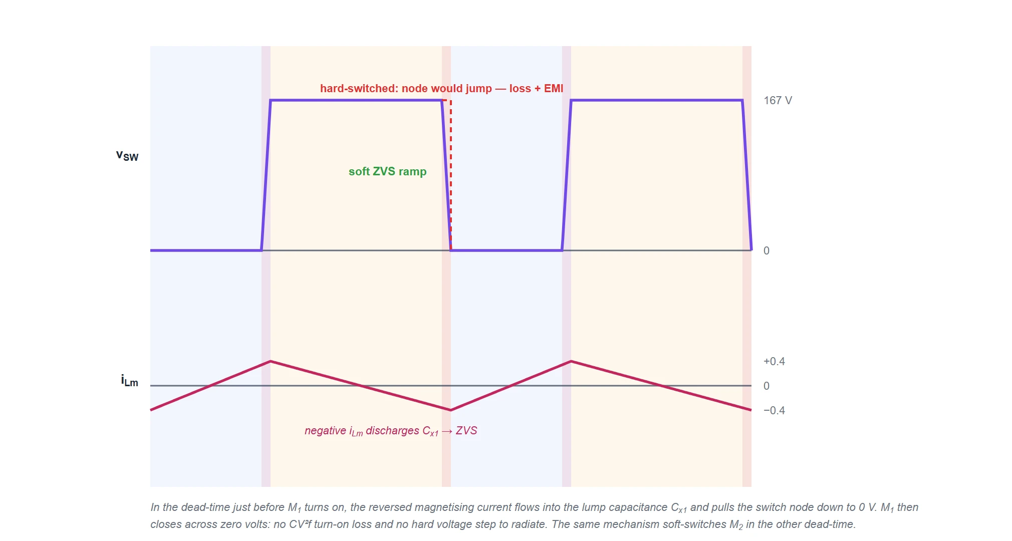
Switching loss in a hard-switched converter comes from turning a device on while there is still voltage across it: the energy ½CxV² stored on the node capacitance is dumped through the channel every cycle, and the abrupt voltage edge radiates EMI. Zero-voltage switching removes both by making sure the voltage is already zero before the channel turns on.
The active clamp arranges exactly that. By letting the magnetising current run negative during the off-time, it keeps a small reservoir of inductive energy that, in the dead-time, flows out of the lump capacitance Cx1 and pulls the switching node smoothly down to ground before M1 is told to turn on. The same thing happens in the other dead-time to soft-switch M2. The energy comes from the leakage and magnetising inductances, so the ZVS condition is essentially “enough inductive energy to discharge the node capacitance”:
½ · Llk · ipk² ≥ ½ · Cx · V² → the node can be swung fully to 0 V within the dead-timeThis is why the magnetising current in an active-clamp forward is deliberately drawn as a bipolar triangle rather than the one-sided ramp of a plain forward: the negative excursion is not a side effect, it is the mechanism.
Waveforms Explained in Detail
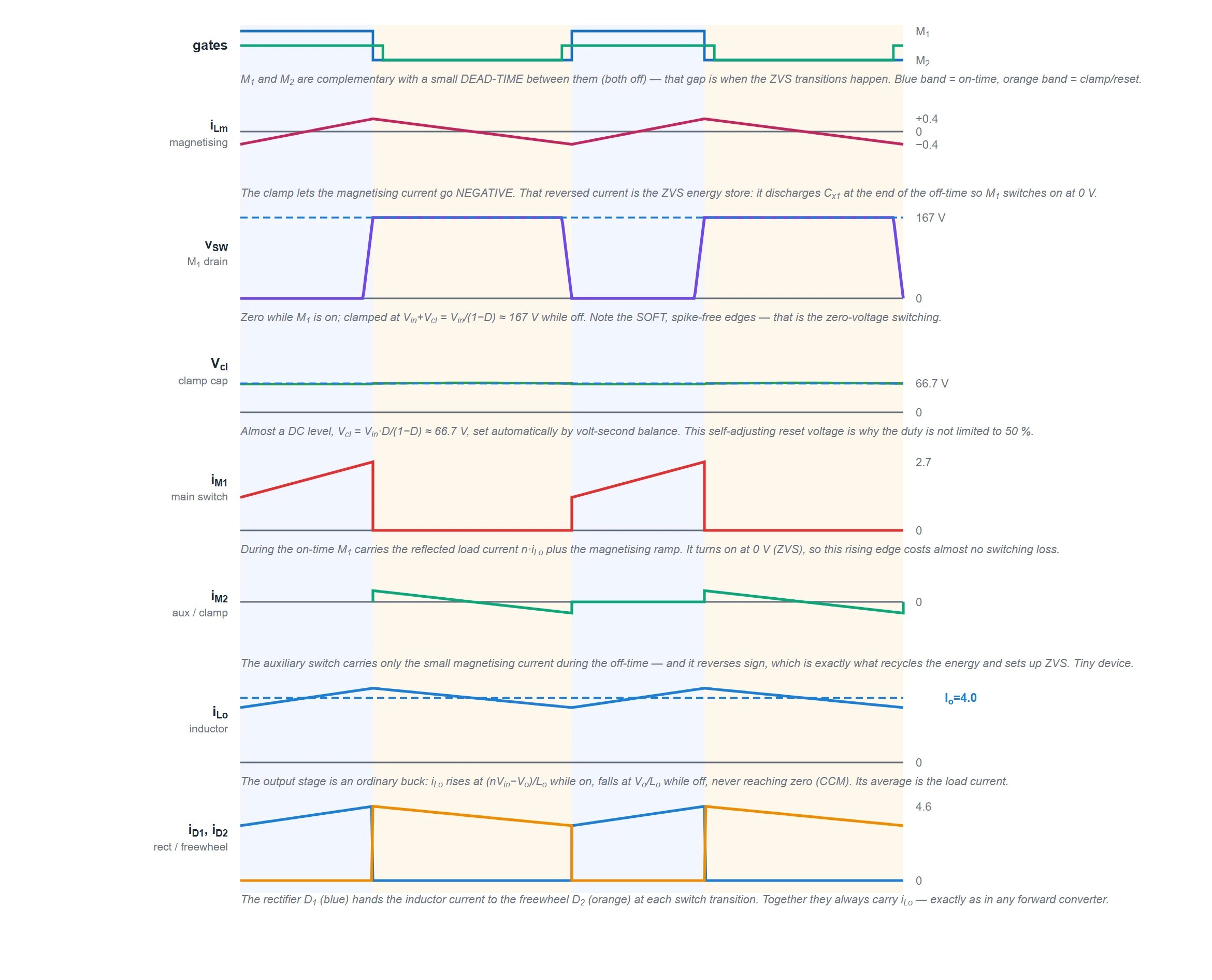
Read the traces together and the converter tells its own story:
- Gates. Two complementary signals, M1 and M2, with a small dead-time between them (both off). Those gaps are short, but they are where the zero-voltage transitions happen.
- Magnetising current iLm. A bipolar triangle: it rises at Vin/Lm during the on-time and is driven down (and negative) at Vcl/Lm during the off-time. The negative part is the ZVS energy store.
- Switch-node voltage vSW. Zero while M1 conducts, then a flat Vin+Vcl = Vin/(1−D) while it is off. Crucially the edges are soft ramps, not vertical jumps — that is the zero-voltage switching, and it means no spike and low EMI.
- Clamp-capacitor voltage Vcl. Almost a DC level, Vin·D/(1−D), with only a small resonant ripple. It sets itself automatically by volt-second balance — the reason the duty is not capped at 50 %.
- Main switch current iM1. The reflected load current plus the magnetising ramp, during the on-time only. Because M1 turns on at 0 V, its leading edge costs almost no switching loss.
- Auxiliary switch current iM2. Only the small magnetising current, during the off-time — and it reverses sign. The auxiliary device is therefore small and lightly loaded; it exists to steer energy, not to carry the load.
- Output inductor current iLo. The ordinary buck ripple: up while on, down while off, never reaching zero (CCM), average equal to the load current. The active clamp changes the primary side, not the output.
- Diode currents iD1, iD2. The rectifier hands the inductor current to the freewheel diode at each transition; together they always carry iLo, just like any forward converter.
Switch Stress & the Duty-Cycle Freedom
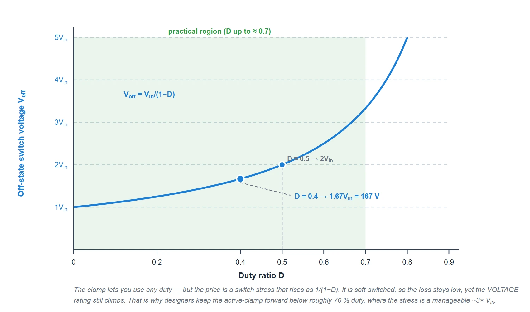
Freedom from the 50 % duty limit is the active clamp’s headline advantage, but it is not free. Because the clamp holds the switching node at Vin + Vcl, and Vcl grows with duty, both MOSFETs must block a voltage that climbs as the duty rises:
Voff = Vin + Vcl = Vin + Vin·D/(1−D) = Vin / (1−D)At D = 0.4 that is 1.67·Vin; at 0.5 it is 2·Vin; at 0.7 it is already 3.3·Vin, and it heads for infinity as the duty approaches one. The switching is soft, so the loss stays low even at high duty, but the voltage rating of the devices still climbs. In practice that is why designers keep an active-clamp forward below roughly 70 % duty, where the stress is a manageable three-times the input. Within that window the converter comfortably covers a 2:1 or wider input range on a single design — something a plain forward cannot do.
Key Formulas
The output side is a buck fed from n·Vin, so the dc transfer follows from volt-second balance, with n = Ns/Np.
Output voltage (CCM) — the same forward law:
(n·Vin − Vo)·D·T = Vo·(1−D)·T → Vo = n · D · VinClamp voltage and switch stress — from volt-second balance on the magnetising inductance (Vin·D = Vcl·(1−D)):
Vcl = Vin · D / (1−D) | Voff,M1 = Voff,M2 = Vin + Vcl = Vin / (1−D)Output-inductor ripple and average:
ΔiLo = (n·Vin − Vo)·D·T / Lo = Vo·(1−D)·T / Lo | ILo,avg = IoMagnetising current (bipolar) and diode stresses:
ΔiLm = Vin·D·T / Lm (peaks ±ΔiLm/2) | VD1 = n·Vcl | VD2 = n·VinZero-voltage-switching condition (enough inductive energy to discharge the node capacitance):
½ · Llk · ipk² ≥ ½ · Cx · Vnode²(Ideal expressions; device drops, dead-times and losses neglected. A well-designed active-clamp forward runs around 92–96 % efficient thanks to the recovered magnetising energy and the zero-voltage turn-on.)
Voltage Gain & Turns Ratio
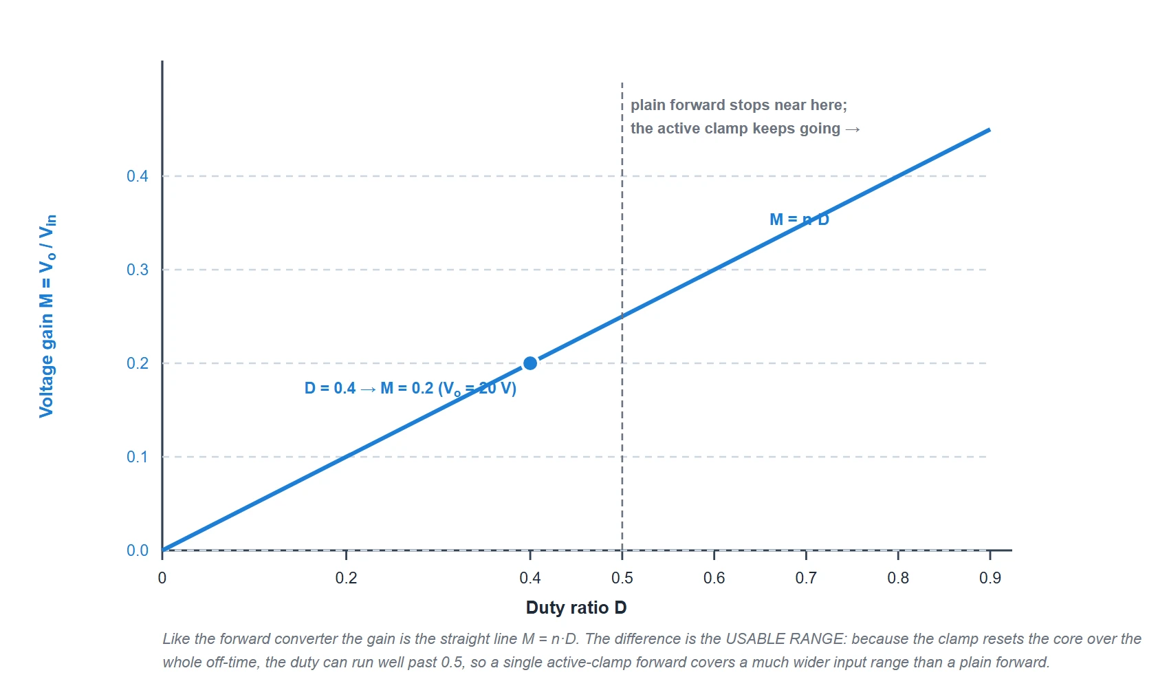
The dc gain is the forward converter’s familiar straight line, M = n·D. Adding the active clamp does not change the transfer function — it changes the usable range of it. Because the clamp resets the core over the whole off-time, the duty can run comfortably past 0.5, so:
- The turns ratio sets the coarse scaling. Choose n for the middle of your input range; the duty then trims around it, and it may sit either side of 0.5 without any reset problem.
- Wide input on one design. A 2:1 input swing simply moves the duty across a range that stays inside the practical ≤ 0.7 window — where a plain forward would have run out of duty margin.
- Light load still means DCM. As in any buck-derived converter, if the output-inductor current reaches zero the output rises above n·D·Vin and becomes load-dependent, so Lo is sized to stay continuous over the working range.
Worked Example
Deliberately the same operating point as our forward and two-switch forward examples, so you can compare the three designs directly.
| Given | Vin = 100 V, Ns:Np = 1:2 (n = 0.5), D = 0.4, f = 50 kHz (T = 20 µs), Lo = 200 µH, Lm = 1 mH |
|---|---|
| Output voltage Vo = n·D·Vin | 0.5 × 0.4 × 100 = 20 V |
| Load (for Io = 4 A) R = Vo/Io, Po | R = 5 Ω, Po = 80 W |
| Clamp voltage Vcl = Vin·D/(1−D) | 100 × 0.4 / 0.6 = 66.7 V |
| Switch stress Voff = Vin/(1−D) | 100 / 0.6 = 166.7 V (= Vin + Vcl) |
| Inductor ripple ΔiLo = Vo(1−D)T/Lo | 20 × 0.6 × 20µ/200µ = 1.2 A (Imax 4.6, Imin 3.4 → CCM) |
| Magnetising ramp ΔiLm = Vin·D·T/Lm | 100 × 0.4 × 20µ/1m = 0.8 A (bipolar, ±0.4 A) |
| Rectifier diode VD1 = n·Vcl | 0.5 × 66.7 = 33.3 V |
| Freewheel diode VD2 = n·Vin | 0.5 × 100 = 50 V |
| Input current (avg) D·(n·Io) | 0.4 × 2 = 0.8 A → Pin = 100 × 0.8 = 80 W = Po ✓ |
Every output-side number is identical to the plain and two-switch forward designs — same 20 V, 4 A, and 1.2 A ripple. The differences are all on the primary: the switch stress is 166.7 V (higher than the two-switch’s hard 100 V, but the switching is now soft), the magnetising current is bipolar (it must reverse for ZVS), and — not shown by a single number — the duty could be pushed well past 0.5 if a wider input range demanded it. That is the active-clamp forward’s bargain: a higher, duty-dependent voltage rating bought back as efficiency and input-range flexibility.
Active-Clamp vs Plain & Two-Switch Forward
| Feature | Plain forward | Two-switch forward | Active-clamp forward |
|---|---|---|---|
| Core reset | Reset winding or RCD snubber | Two clamp diodes to the rails | Active clamp (Ccl + M2) |
| Reset energy | Burned (snubber) or returned (winding) | Returned to the input | Recycled resonantly |
| Switching | Hard | Hard | Soft (ZVS) |
| Switch stress | ≈ 2Vin + leakage spike | Vin (hard-clamped) | Vin/(1−D), duty-dependent |
| Duty limit | D ≤ 0.5 (typ.) | D ≤ 0.5 (fixed) | No 0.5 limit (keep ≲ 0.7 for stress) |
| Switches | 1 | 2, driven together | 2, driven out of phase |
| Gain | Vo = n·D·Vin — identical for all three | ||
| Efficiency / EMI | Lower / higher EMI | Good / low ringing | Highest / lowest EMI |
| Best for | Simple, low cost | High-voltage buses, rugged | Efficiency, wide input, low EMI |
Advantages & Disadvantages
Advantages
- Zero-voltage switching of both transistors — turn-on switching loss is essentially eliminated, so the converter can run at high frequency with high efficiency (typically 92–96 %).
- Magnetising energy is recycled, not burned in a snubber — less heat, higher efficiency, no dissipative reset network.
- No 50 % duty limit. The self-adjusting clamp voltage resets the core over the whole off-time, so one design can cover a wide input range.
- Low EMI. The soft, spike-free switching edges radiate far less than a hard-switched forward, easing filtering and compliance.
- No reset winding. An ordinary two-winding transformer; the clamp does the reset job.
- Small auxiliary switch. M2 only ever carries the tiny magnetising current, so it is a low-cost device.
Disadvantages
- Duty-dependent switch stress Vin/(1−D) — higher-voltage MOSFETs are needed than in a two-switch forward, and the rating climbs steeply if the duty is allowed too high.
- More complex control. Complementary drive with a carefully set dead-time is required — too little and you lose ZVS, too much and the body diodes conduct and lose efficiency.
- ZVS is load-dependent. At very light load there may not be enough inductive energy to fully discharge the node capacitance, so the soft-switching benefit fades (mitigated by design or by adding magnetising current).
- An extra switch and its floating gate drive, plus the clamp capacitor — more parts than a single-switch forward.
- The clamp capacitor sees the full magnetising ripple, so it must be a good low-ESR film part rated for the clamp voltage.
Applications
- On-board and point-of-load converters for telecom and data-computing systems, where high efficiency in a small size is the priority — the classic active-clamp forward use case.
- 48 V and high-voltage-DC distribution supplies feeding low-voltage, high-current loads, where the ZVS efficiency and self-driven synchronous rectification pay off.
- Wide-input industrial and instrumentation supplies, which exploit the freedom from the 50 % duty limit to cover a 2:1 or wider input range on one design.
- Low-EMI supplies in audio, medical and RF-sensitive equipment, where the soft switching keeps radiated noise low.
- Adapters and auxiliary supplies in the tens-to-few-hundred-watt range where efficiency standards are tight.
- Anywhere a forward converter needs higher efficiency without moving to a full bridge — the active clamp is the natural single-switch-stage upgrade.
The rule of thumb: reach for the active-clamp forward when efficiency, input range and EMI matter more than the absolute simplicity of a plain forward or the rugged high-voltage clamping of a two-switch forward. At higher power a full-bridge or phase-shifted full-bridge takes over.
Frequently Asked Questions – FAQs
Related Topics
- Forward Converter — the single-switch original
- Two-Switch Forward Converter — hard-clamped and rugged
- Flyback Converter — the low-power isolated buck-boost
- Full-Bridge Converter — the high-power step up
- Buck Converter (Step-Down) — the non-isolated parent
- MOSFET — the switch and its body diode
- All Power Electronic Converters