Depletion Region
The complete guide to the depletion region — the carrier-free space-charge zone at the heart of every PN junction. From how it forms by diffusion and recombination, to the built-in barrier potential, forward vs reverse bias, and junction capacitance.
Complete Learning Path — Depletion Region
From how the depletion region forms, through the barrier potential and bias effects, to its charge/field/potential profile, width and junction capacitance
What is the Depletion Region?
The depletion region — also called the space-charge region or depletion layer — is the thin zone around a PN junction that is emptied of free charge carriers. It is the feature that makes a diode a diode.
When a P-type region (rich in holes) meets an N-type region (rich in electrons), carriers diffuse across the junction and recombine. Left behind are the fixed, charged dopant ions — negative acceptors on the P side, positive donors on the N side — a region with charge but no free carriers.
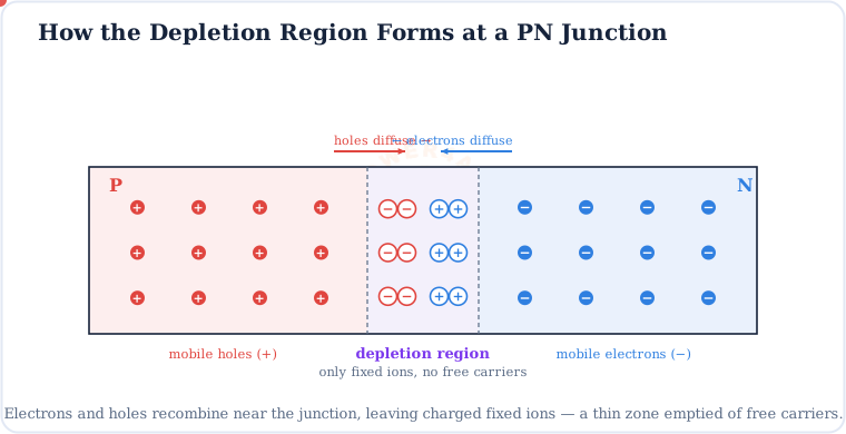
Space charge, but no current
The depletion region contains charged fixed ions but no mobile carriers, so it behaves like an insulating barrier — until an applied voltage changes its width.
Built-in Field & Barrier Potential
Those fixed ions create an internal electric field across the depletion region and a barrier potential that opposes further diffusion — the equilibrium that stabilises the junction.

Vbi = (kT/q) ln(NAND / ni²) · ≈ 0.7 V (Si), 0.3 V (Ge)
Built-in (barrier) potential from the doping levels; k = Boltzmann, T = temperature, q = electron charge
Why a diode “turns on” at 0.7 V
The barrier potential is exactly the forward voltage a silicon diode needs before it conducts strongly — the famous 0.7 V knee.
Forward Bias: the Region Narrows
Connect the battery + to P and − to N and you fight the built-in field. Majority carriers are pushed toward the junction, so the depletion region narrows and the barrier falls.
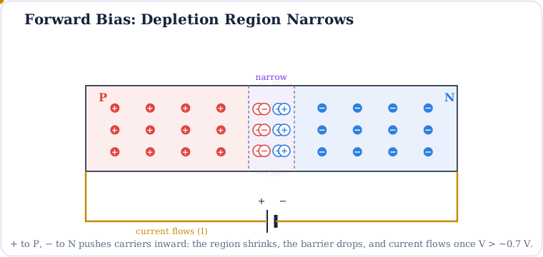
This is how a diode conducts
A forward-biased junction is a low-resistance path — the basis of rectification, LEDs and the “on” state of transistors.
Reverse Bias: the Region Widens
Reverse the battery — + to N and − to P — and you reinforce the built-in field. Carriers are pulled away from the junction, so the depletion region widens and the barrier rises. Almost no current flows.

Breakdown
Push reverse voltage too high and the junction breaks down (avalanche or Zener effect), conducting suddenly — deliberately exploited in Zener diodes for voltage regulation.
Charge, Field & Potential Profile
Three graphs across the depletion width tell the whole quantitative story — from fixed charge, to the field it creates, to the potential that results.

Emax at the junction · area under E = Vbi · NAxP = NDxN
Charge neutrality makes the region extend further into the lightly-doped side
Depletion Width & Junction Capacitance
The width W changes with doping and bias — and because the region separates charge like a capacitor, it gives the junction a voltage-controlled capacitance.

W ∝ √(Vbi − V) · Cj = εA / W ∝ 1/√(Vbi − V)
Depletion width and junction (transition) capacitance vs applied voltage
The varactor diode
A reverse-biased junction is a voltage-tunable capacitor — the varactor (varicap) diode, used to tune radios, PLLs and oscillators electronically.
Why the Depletion Region Matters
Almost every semiconductor device works by controlling a depletion region.
Diodes & rectifiers
Its one-way behaviour turns AC into DC in every diode and rectifier.
LEDs & lasers
Recombination across the junction emits light in LEDs and laser diodes.
Solar cells & photodiodes
The built-in field sweeps light-generated carriers apart to make current.
Varactors
Voltage-controlled junction capacitance tunes RF circuits.
Zener & breakdown
Controlled reverse breakdown regulates voltage in Zener diodes.
Key Terms at a Glance
The essential depletion-region vocabulary students and engineers search for.
Depletion region
Carrier-free space-charge zone at a junction.
Space charge
Fixed acceptor (−) & donor (+) ions.
Barrier potential
Vbi ≈ 0.7 V (Si), 0.3 V (Ge).
Built-in field
Internal field N → P.
Depletion width W
Thickness; changes with bias.
Forward / reverse bias
Narrows / widens the region.
Junction capacitance
Cj = εA/W.
Leakage current
Tiny reverse IS.
Frequently Asked Questions
Quick, expert answers to the questions people ask most about the depletion region.
What is the depletion region in simple words?
It is a thin layer around a PN junction with no free electrons or holes — only fixed charged ions. Because it has no free carriers, it acts like a barrier that controls whether the diode conducts.
How is the depletion region formed?
Electrons from the N side and holes from the P side diffuse across the junction and recombine, leaving fixed donor and acceptor ions. Their charge builds a field that stops further diffusion, forming a stable carrier-free zone.
What is the barrier potential?
The voltage across the depletion region from the fixed ions: about 0.7 V for silicon and 0.3 V for germanium. A forward voltage must exceed it before the diode conducts.
Does forward bias increase or decrease the depletion region?
Forward bias decreases (narrows) it. Pushing carriers toward the junction lowers the barrier, so above ~0.7 V the diode conducts.
Why does reverse bias widen the depletion region?
Reverse bias pulls majority carriers away from the junction, exposing more fixed ions, so the region grows wider and the barrier gets higher — blocking current except a tiny leakage.
What is the depletion width?
The thickness W of the region. It depends on doping and voltage, extends further into the lightly-doped side, and roughly follows W ∝ √(Vbi − V).
What is junction (depletion) capacitance?
The capacitance from charge stored across the depletion region, Cj = εA/W. Since reverse bias widens W, the capacitance falls — a voltage-controlled capacitor (varactor).
Is there current in the depletion region?
At equilibrium, essentially no net current — diffusion and drift balance. It has fixed charge but no free carriers, so it behaves like an insulator until bias changes its width.
Conclusion & Key Takeaways
The depletion region is the small carrier-free zone that gives the PN junction — and all of modern electronics — its one-way behaviour.
Carrier-free zone
Fixed ions only.
Barrier Vbi
0.7 V Si, 0.3 V Ge.
Forward → narrows
Diode conducts.
Reverse → widens
Blocks current.
Width W
∝ √(Vbi − V).
Cj = εA/W
Voltage-tunable (varactor).