P-Type & N-Type Doping
How a pinch of impurity turns a pure crystal into an engineered conductor. Learn n-type doping (pentavalent donors), p-type doping (trivalent acceptors), donor & acceptor ionization, the dopant elements, the doping methods (diffusion, ion implantation, epitaxy) and doping levels — the step that follows intrinsic & extrinsic semiconductors and leads to the PN junction.
Complete Learning Path — P-Type & N-Type Doping
From what doping is, to donors & acceptors, dopant elements, doping methods, doping levels and the n vs p comparison
What Is Doping?
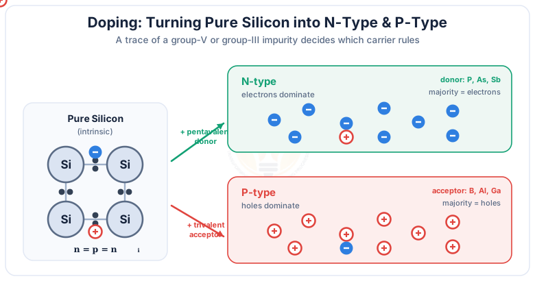
Doping is the deliberate addition of a tiny, controlled amount of impurity to a pure semiconductor to raise and precisely control its conductivity. It is the single step that turns useless-on-its-own silicon into the n-type and p-type material that builds every diode, transistor and chip.
A pure (intrinsic) semiconductor has very few carriers, so it barely conducts and its conductivity swings wildly with temperature. Doping fixes both problems at once: it injects a large, stable supply of one carrier type. Add a group-V atom with a spare electron and you get n-type; add a group-III atom that is short an electron and you get p-type.
New here?
If you want the big picture of pure vs doped material first, start with Intrinsic & Extrinsic Semiconductors. This page zooms in on the doping step itself — the impurities, the methods and the levels.
N-Type Doping (Pentavalent Donor)
N-type doping adds a pentavalent group-V atom — phosphorus, arsenic or antimony. Four of its five valence electrons bond with the silicon; the fifth is barely held and breaks free, so the donor ionizes and the crystal gains a conduction electron.
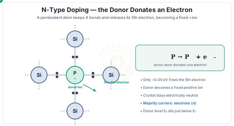
P → P+ + e−. It takes only ~0.05 eV to free the 5th electron, so at room temperature nearly every donor is ionized — electrons become the majority carrier.The free-electron concentration n roughly equals the donor concentration ND, because almost all donors give up their electron. The material is called n-type because the majority carriers are negative electrons — yet it stays electrically neutral, since each donor is left as a fixed positive ion.
P-Type Doping (Trivalent Acceptor)
P-type doping adds a trivalent group-III atom — boron, aluminium or gallium. With only three valence electrons it leaves one bond incomplete; a neighbouring electron hops in to complete it, so the acceptor ionizes and a mobile hole is created.
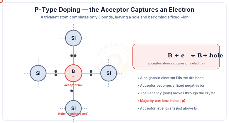
B + e− → B− + hole. The acceptor captures an electron to complete its fourth bond, becoming a fixed negative ion, and the vacancy (hole) drifts away as the majority carrier.The hole concentration p roughly equals the acceptor concentration NA. The material is called p-type because the majority carriers are effectively positive holes — and again it stays neutral, since each acceptor becomes a fixed negative ion.
Dopant Elements — Group III & Group V
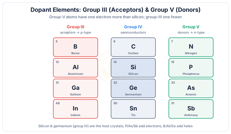
Which impurity you choose decides everything. It comes straight from the periodic table: silicon sits in group IV with four valence electrons, so its neighbours to either side are the dopants.
Group V — donors
Phosphorus, arsenic, antimony: 5 valence electrons, one to spare → n-type.
Group III — acceptors
Boron, aluminium, gallium: 3 valence electrons, one short → p-type.
Group IV — host
Silicon & germanium: 4 valence electrons, the crystal being doped.
Compound hosts
GaAs, GaN and SiC are doped with their own donor/acceptor sets for LEDs and power devices.
How Doping Is Done
Doping is a manufacturing step. Three methods put the impurity exactly where it is needed: thermal diffusion, ion implantation and epitaxy.
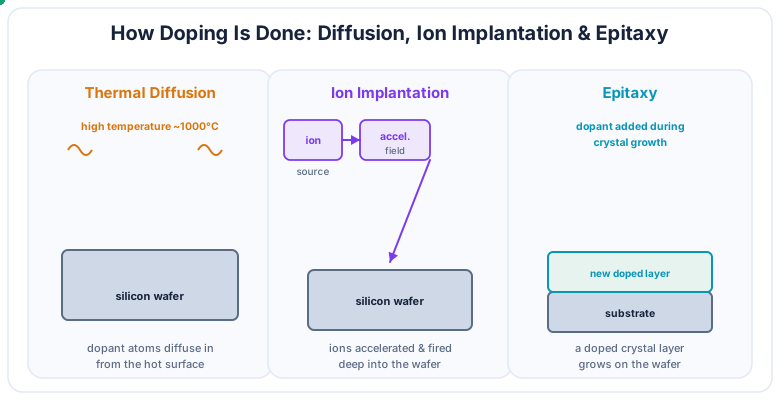
| Method | How it works | Strength |
|---|---|---|
| Thermal diffusion | Dopant diffuses into a wafer heated to ~1000 °C | Simple, cheap, deep junctions |
| Ion implantation | Dopant ions accelerated and fired into the surface | Very precise dose & depth |
| Epitaxy | A doped crystal layer is grown on the substrate | Ultra-clean, controlled layers |
| Alloying | A doped metal is fused into the surface (older method) | Simple contacts / junctions |
Doping Concentration & Levels
How much you dope matters as much as what you dope with. Doping density sets the carrier count — and therefore the resistivity — from lightly doped to almost metallic.
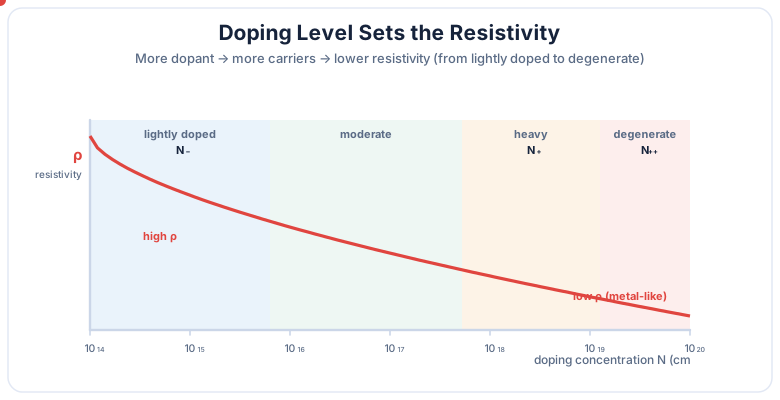
Resistivity ρ is inversely proportional to the doping concentration N (with charge q and mobility μ). More dopant → more carriers → lower resistivity. Notation: N−/P− = lightly doped; N+/P+ = heavily doped (used for low-resistance contacts).
Compensation
If a region has both donors and acceptors, they partly cancel — the net excess decides the type. Deliberately overdoping a p-type region with donors flips it to n-type, which is exactly how a PN junction is written into the silicon.
N-Type vs P-Type Doping
The two doping types are mirror images. Here they are side by side.
| Feature | N-Type Doping | P-Type Doping |
|---|---|---|
| Dopant group | Pentavalent (group V) | Trivalent (group III) |
| Common dopants | P, As, Sb | B, Al, Ga |
| Impurity role | Donor | Acceptor |
| Ionizes to | Fixed positive ion | Fixed negative ion |
| Majority carrier | Electrons (−) | Holes (+) |
| Minority carrier | Holes | Electrons |
| Carrier count | n ≈ ND | p ≈ NA |
| Impurity level | Donor level just below Ec | Acceptor level just above Ev |
| Fermi level | Near conduction band | Near valence band |
| Net charge | Neutral | Neutral |
From Doping to the PN Junction
Doping is not the destination — it is the tool. Put a p-type region next to an n-type region in the same crystal and you create the most important structure in electronics: the PN junction.
At the boundary, electrons and holes diffuse across and recombine, leaving a depletion region of fixed donor and acceptor ions with a built-in voltage. That is what makes a junction conduct in one direction only. Every diode, every transistor, every solar cell and LED is built from doped n- and p-regions arranged in clever patterns — which is why doping is the foundation of all power electronics and microelectronics.
The takeaway
Master n-type and p-type doping and the PN junction, the BJT, the MOSFET and the whole chip suddenly make sense — they are all just doped regions in silicon.
Applications
Controlled doping is the reason modern electronics exists at all.
Diodes & rectifiers
A doped p–n boundary conducts one way — the diode.
Transistors & ICs
Patterned n- and p-regions form BJTs, MOSFETs and billions-strong chips.
LEDs & lasers
Doped compound semiconductors emit light at a junction.
Solar cells
A large doped junction separates light-generated carriers into current.
Ohmic contacts
Heavily doped N+/P+ regions make low-resistance metal contacts.
Power devices
Doped Si, SiC and GaN switch high power in converters and drives.
Key Terms at a Glance
The essential doping vocabulary students and engineers search for.
Doping
Adding controlled impurity to a semiconductor.
Donor
Pentavalent atom; gives an electron (n-type).
Acceptor
Trivalent atom; makes a hole (p-type).
Ionization
Dopant giving up / capturing an electron.
N+ / N−
Heavily / lightly doped notation.
Degenerate
So heavily doped it conducts like metal.
Frequently Asked Questions
Quick, exam-ready answers to the questions people ask most about p-type and n-type doping.
What is doping in a semiconductor?
Doping is the deliberate addition of a tiny, controlled amount of impurity atoms to a pure semiconductor to raise and control its conductivity. Typical levels are about one impurity atom in a million to a hundred million semiconductor atoms, which is enough to increase conductivity by many orders of magnitude and to decide whether the material is n-type or p-type.
What is n-type doping?
N-type doping adds a pentavalent group-V impurity such as phosphorus, arsenic or antimony to silicon. Four of the impurity's five valence electrons form covalent bonds and the fifth is easily released, so the donor ionizes to a fixed positive ion and gives a free conduction electron. Electrons become the majority carriers, so the material is negative-type, or n-type.
What is p-type doping?
P-type doping adds a trivalent group-III impurity such as boron, aluminium or gallium to silicon. With only three valence electrons the acceptor completes just three bonds; the fourth bond captures an electron from a neighbour, so the acceptor ionizes to a fixed negative ion and leaves a mobile hole. Holes become the majority carriers, so the material is positive-type, or p-type.
What is the difference between a donor and an acceptor?
A donor is a pentavalent impurity that donates a free electron and makes an n-type semiconductor; its energy level sits just below the conduction band and it becomes a fixed positive ion when ionized. An acceptor is a trivalent impurity that accepts an electron, creates a hole and makes a p-type semiconductor; its level sits just above the valence band and it becomes a fixed negative ion.
Which elements are used as dopants?
Donors are group-V elements: phosphorus, arsenic and antimony. Acceptors are group-III elements: boron, aluminium, gallium and indium. The host crystals are the group-IV semiconductors silicon and germanium, which have four valence electrons, so a group-V atom brings one extra electron and a group-III atom is short by one.
What are the main methods of doping?
The three main methods are thermal diffusion, in which dopant atoms diffuse into a heated wafer from a gas at around a thousand degrees Celsius; ion implantation, in which dopant atoms are ionized, accelerated and fired as a beam deep into the wafer for precise control; and epitaxy, in which a new doped crystal layer is grown on the wafer with the dopant added during growth.
What is donor and acceptor ionization?
Ionization is when the dopant gives up or captures an electron. A donor needs only about 0.05 electron-volts to release its extra electron, becoming a positive ion, so at room temperature almost all donors are ionized. An acceptor captures an electron to complete its bond, becoming a negative ion and releasing a hole. In both cases the crystal stays electrically neutral overall.
Does doping change the charge of the semiconductor?
No. Doping does not add net charge. In n-type material each donor that gives up an electron becomes a fixed positive ion that balances the mobile electron, and in p-type material each acceptor becomes a fixed negative ion that balances the mobile hole, so the crystal remains electrically neutral.
What is a heavily doped or degenerate semiconductor?
Doping levels are described from lightly doped, written N minus, through moderate and heavily doped, written N plus, to degenerate, written N plus plus. A heavily doped or degenerate semiconductor has so many dopant atoms, above about ten to the nineteenth per cubic centimetre, that its Fermi level enters the conduction or valence band and it conducts almost like a metal; such regions are used for ohmic contacts.
How does doping affect resistivity and conductivity?
Doping adds free carriers, so conductivity rises and resistivity falls as the doping concentration increases, roughly as resistivity equals one over the product of charge, carrier concentration and mobility. Raising the doping from lightly doped to degenerate can cut the resistivity by many orders of magnitude.
What is compensation doping?
Compensation is when a semiconductor contains both donors and acceptors. The two partly cancel: the net carrier type is set by whichever is in excess, so if donors exceed acceptors the material is n-type with a net donor concentration equal to the difference. Overdoping a p-type region with donors can convert it to n-type, which is how junctions are formed.
Why is silicon doped instead of used pure?
Pure (intrinsic) silicon has very few carriers and a conductivity that changes strongly and unpredictably with temperature. Doping provides a large, stable and controllable number of one carrier type, which is essential to make diodes, transistors and integrated circuits with predictable behaviour.
Conclusion & Key Takeaways
P-type and n-type doping is the deliberate, precise act that gives silicon its electrical personality — a donor for electrons, an acceptor for holes, dosed and placed exactly where a device needs it.
N-type
Pentavalent donor → electrons.
P-type
Trivalent acceptor → holes.
Ionization
Donor → +ion, acceptor → −ion.
Methods
Diffusion, implant, epitaxy.
Level sets ρ
N− to degenerate N++.
Builds junctions
p + n = the diode.