Intrinsic & Extrinsic Semiconductors
Pure vs doped — the two faces of every semiconductor. Learn what an intrinsic (pure) semiconductor is, how covalent bonds and electron–hole pairs work, the energy band gap and Fermi level, how doping makes extrinsic semiconductors, and the difference between n-type and p-type — the foundation of every diode and transistor.
Complete Learning Path — Intrinsic & Extrinsic Semiconductors
From the pure silicon lattice and energy bands, to doping, n-type & p-type, carriers and applications
Intrinsic vs Extrinsic Semiconductors
A semiconductor is a material whose conductivity sits between a conductor and an insulator — and it comes in two forms. An intrinsic semiconductor is pure; an extrinsic semiconductor is doped with a trace of impurity to control how it conducts.
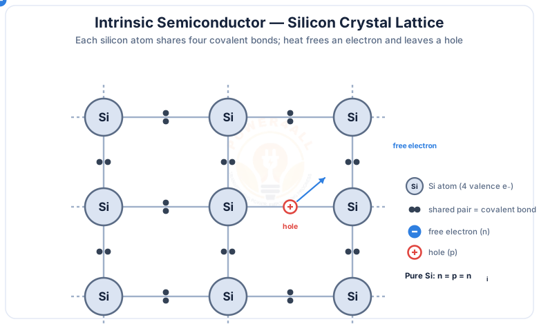
In a pure crystal of silicon (Si) or germanium (Ge), every atom has four valence electrons and shares a covalent bond with each of its four neighbours. That is the intrinsic material. By adding the right impurity — a process called doping — we turn it into an extrinsic semiconductor with a huge, controllable supply of one carrier type, which is exactly what makes diodes, transistors and chips possible.
n = p = ni.The one-line idea
Pure semiconductor = equal electrons and holes, poor conductor. Add a pinch of the right impurity and you flood it with one carrier — turning a mediocre conductor into a precisely engineered one.
Intrinsic (Pure) Semiconductors
In an intrinsic semiconductor the only charge carriers come from thermal breaking of covalent bonds. Each broken bond makes one free electron and one hole — a matched pair.
At absolute zero a pure crystal is a perfect insulator: every electron is locked in a bond. As temperature rises, thermal energy frees electrons; each departure leaves a hole (a missing electron that behaves like a positive charge). Neighbouring electrons hop into holes, so holes drift too. Because pairs are created together, the electron and hole counts stay equal: n = p = ni, the intrinsic carrier concentration.
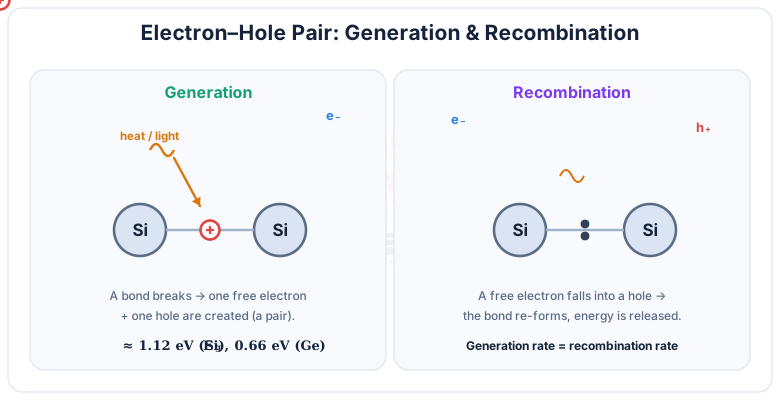
In a pure semiconductor the free-electron concentration n equals the hole concentration p, both equal to the intrinsic carrier concentration ni. For silicon ni ≈ 1.5 × 1010 cm−3 at 300 K — tiny, so pure silicon barely conducts.
Strongly temperature-dependent
ni rises sharply with temperature, roughly as ni ∝ T3/2 e−Eg/2kT. That is why an intrinsic semiconductor's conductivity climbs with heat — the opposite of a metal — and why practical devices use doping instead of relying on temperature.
Energy Bands, the Band Gap & the Fermi Level
The clearest way to see why semiconductors behave as they do is the energy band diagram: a filled valence band, an empty conduction band, and a forbidden band gap between them.
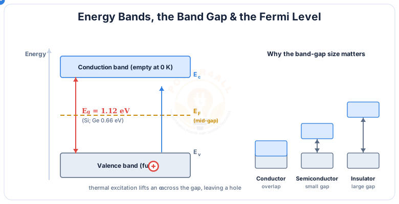
≥ Eg to jump from the valence band to the conduction band, leaving a hole. The Fermi level sits mid-gap for intrinsic material. A conductor's bands overlap; an insulator's gap is huge.An electron can only conduct once it reaches the conduction band. The energy needed is the band gap Eg: about 1.12 eV for silicon and 0.66 eV for germanium. A conductor has overlapping bands (no gap), an insulator has a very large gap (> 3 eV), and a semiconductor's small gap is exactly what lets modest heat, light or an applied field control its conduction. The Fermi level (EF) — the reference energy for the probability of occupied states — lies near the middle of the gap in an intrinsic semiconductor, and doping shifts it, as we will see.
Doping: Making Extrinsic Semiconductors
Pure silicon is a poor conductor. Doping — adding a controlled trace of impurity — floods it with one carrier type and creates an extrinsic semiconductor whose conductivity we can set by design.
The amount is tiny — typically one impurity atom in 106 to 108 silicon atoms — yet it can raise conductivity by many orders of magnitude. There are two flavours, decided entirely by whether the impurity has one electron too many or one too few compared with silicon's four:
N-type — pentavalent donor
Group-V atoms (P, As, Sb) have 5 valence electrons; the spare one becomes a free electron. Majority carriers: electrons.
P-type — trivalent acceptor
Group-III atoms (B, Al, Ga) have 3 valence electrons; the missing bond is a hole. Majority carriers: holes.
Still neutral overall
Doping does not add charge. A donor that gives up its electron becomes a fixed positive ion; an acceptor that grabs one becomes a fixed negative ion. The mobile carriers move, but the crystal stays electrically neutral.
N-Type Semiconductor (Pentavalent Donor)
Dope silicon with a pentavalent group-V atom — phosphorus, arsenic or antimony — and you get an n-type semiconductor, where electrons are the majority carriers.
The donor has five valence electrons. Four form covalent bonds with the surrounding silicon; the fifth is only loosely held and, at room temperature, is easily freed to roam the crystal. Each donor thus donates one conduction electron without creating a hole. The result: many free electrons (majority), few holes (minority), and a Fermi level that shifts up toward the conduction band.
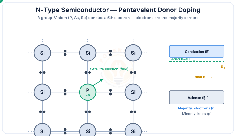
EF moves up near Ec.With donor concentration ND, the majority electron concentration is roughly ND, and the minority hole concentration falls to ni2/ND by the mass-action law. Doping electrons up pushes holes down.
P-Type Semiconductor (Trivalent Acceptor)
Dope silicon with a trivalent group-III atom — boron, aluminium or gallium — and you get a p-type semiconductor, where holes are the majority carriers.
The acceptor has only three valence electrons, so it can complete just three of the four bonds around it. The fourth bond is left short of an electron — a hole. A nearby electron soon hops in to complete that bond (the acceptor accepts it), passing the hole along. The result: many holes (majority), few electrons (minority), and a Fermi level that shifts down toward the valence band.
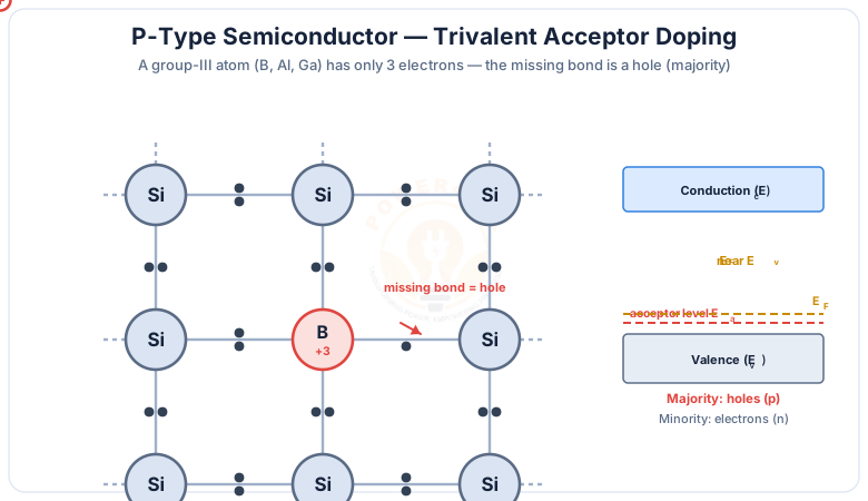
EF moves down near Ev.With acceptor concentration NA, the majority hole concentration is roughly NA, and the minority electron concentration is ni2/NA. Join a p-type and an n-type region and you have a PN junction — the heart of the diode.
Intrinsic vs Extrinsic — and N-Type vs P-Type
Here is the whole picture at a glance: pure vs doped, and the two doped types side by side.
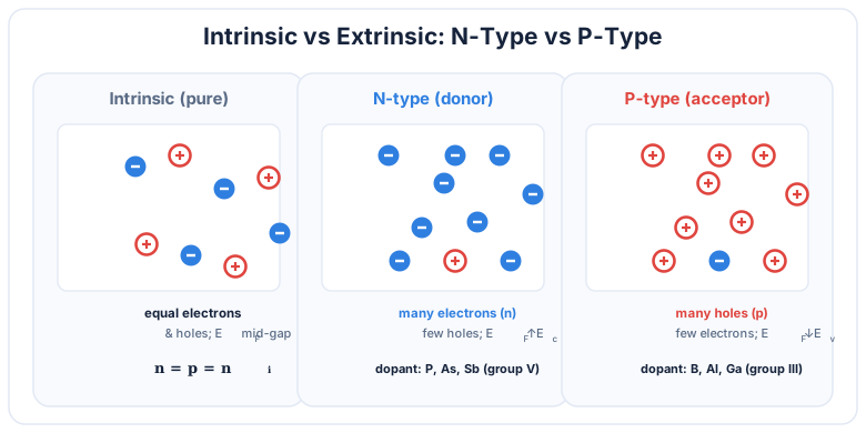
| Property | Intrinsic | N-type | P-type |
|---|---|---|---|
| Purity | Pure Si / Ge | Doped (pentavalent) | Doped (trivalent) |
| Dopant | None | P, As, Sb (group V) | B, Al, Ga (group III) |
| Impurity role | — | Donor | Acceptor |
| Majority carrier | e− = holes | Electrons | Holes |
| Minority carrier | — | Holes | Electrons |
| n vs p | n = p = ni | n ≫ p | p ≫ n |
| Fermi level | Mid-gap | Near conduction band | Near valence band |
| Conductivity | Low, temperature-driven | High, controllable | High, controllable |
Carriers, Conductivity & the Mass-Action Law
Both electrons and holes carry current, and a single elegant law ties their numbers together in any semiconductor at equilibrium.
The mass-action law: at a given temperature the product of electron and hole concentrations is constant, equal to ni2. So raising one carrier by doping automatically lowers the other — the product never changes.
Conductivity σ adds the contribution of both carriers: charge q, concentrations n and p, and mobilities μn and μp. Electrons move faster than holes, so n-type material of the same doping conducts a little better.
Worked example — minority carriers
Silicon (ni = 1.5 × 1010 cm−3) is doped n-type with ND = 1 × 1016 cm−3. Then n ≈ 1016, and the minority holes are p = ni2/ND = (1.5×10¹⁰)2 / 1016 ≈ 2.25 × 104 cm−3 — about a trillion times fewer than the electrons. That is why we call them minority carriers.
Applications
Doped semiconductors are the raw material of all modern electronics — every junction is just p-type meeting n-type.
Diodes & rectifiers
A single PN junction of p-type and n-type silicon conducts one way only.
Transistors & ICs
BJTs and MOSFETs stack n- and p-regions; billions form every microchip.
LEDs & lasers
Electrons and holes recombine across a junction and emit light.
Solar cells
Light generates electron–hole pairs that a junction separates into current.
Sensors & thermistors
Carrier counts change with heat, light or strain — the basis of many sensors.
Power electronics
Doped Si, SiC and GaN switch high power in converters and drives.
Key Terms at a Glance
The essential intrinsic & extrinsic semiconductor vocabulary students search for.
Intrinsic
Pure semiconductor; n = p = ni.
Extrinsic
Doped semiconductor (n- or p-type).
Donor / Acceptor
Pentavalent (gives e−) / trivalent (gives hole).
Majority / minority
The more / less numerous carrier.
Band gap Eg
Energy to reach the conduction band.
Fermi level EF
Reference energy; shifts with doping.
Frequently Asked Questions
Quick, exam-ready answers to the questions people ask most about intrinsic and extrinsic semiconductors.
What is an intrinsic semiconductor?
An intrinsic semiconductor is a pure semiconductor crystal, such as silicon or germanium, with no added impurity. Every atom forms four covalent bonds with its neighbours. Thermal energy breaks a few bonds, creating equal numbers of free electrons and holes, so n equals p equals the intrinsic carrier concentration ni.
What is an extrinsic semiconductor?
An extrinsic semiconductor is a semiconductor that has been doped, meaning a small controlled amount of impurity has been added to greatly increase its conductivity. Doping with a pentavalent donor makes an n-type semiconductor with electrons as majority carriers; doping with a trivalent acceptor makes a p-type semiconductor with holes as majority carriers.
What is the difference between intrinsic and extrinsic semiconductors?
An intrinsic semiconductor is pure and has equal numbers of electrons and holes with low conductivity that depends strongly on temperature. An extrinsic semiconductor is doped, so it has far more of one carrier type, much higher and more controllable conductivity, and a Fermi level shifted toward the conduction band (n-type) or the valence band (p-type).
What is doping in a semiconductor?
Doping is the deliberate addition of a tiny, controlled amount of impurity atoms to a pure semiconductor to change its electrical properties. Typical doping levels are about one impurity atom in a million to a hundred million semiconductor atoms, which is enough to raise conductivity by many orders of magnitude and to fix whether the material is n-type or p-type.
What is an n-type semiconductor?
An n-type semiconductor is made by doping with a pentavalent group-V impurity such as phosphorus, arsenic or antimony. The impurity has five valence electrons; four form covalent bonds and the fifth is easily freed, so it donates a conduction electron. Electrons are the majority carriers and holes the minority carriers, and the Fermi level moves up toward the conduction band.
What is a p-type semiconductor?
A p-type semiconductor is made by doping with a trivalent group-III impurity such as boron, aluminium or gallium. The impurity has only three valence electrons, so one covalent bond is left incomplete, creating a hole that accepts an electron. Holes are the majority carriers and electrons the minority carriers, and the Fermi level moves down toward the valence band.
What are majority and minority carriers?
Majority carriers are the more numerous charge carriers in an extrinsic semiconductor: electrons in n-type and holes in p-type. Minority carriers are the less numerous type: holes in n-type and electrons in p-type. Their concentrations are linked by the mass-action law, n times p equals ni squared.
What is the difference between a donor and an acceptor?
A donor is a pentavalent impurity that donates a free electron and creates an n-type semiconductor; its energy level sits just below the conduction band. An acceptor is a trivalent impurity that accepts an electron, creating a hole and a p-type semiconductor; its energy level sits just above the valence band.
What is the energy band gap of silicon and germanium?
The band gap is the forbidden energy range between the valence band and the conduction band. Silicon has a band gap of about 1.12 electron-volts and germanium about 0.66 electron-volts at room temperature. A conductor has overlapping bands with no gap, and an insulator has a very large gap, which is why semiconductors sit between the two.
Where is the Fermi level in intrinsic, n-type and p-type semiconductors?
In an intrinsic semiconductor the Fermi level lies near the middle of the band gap. In an n-type semiconductor it shifts up toward the conduction band because of the extra electrons, and in a p-type semiconductor it shifts down toward the valence band because of the extra holes.
What is the mass-action law for semiconductors?
The mass-action law states that, at thermal equilibrium, the product of the electron and hole concentrations is constant for a given material and temperature: n times p equals ni squared, where ni is the intrinsic carrier concentration. So doping that raises one carrier type automatically lowers the other, keeping the product fixed.
Are extrinsic semiconductors electrically charged?
No. Even though n-type has extra electrons and p-type has extra holes, both are electrically neutral overall. Each donor that gives up an electron becomes a fixed positive ion, and each acceptor that gains an electron becomes a fixed negative ion, so the total charge stays balanced.
Conclusion & Key Takeaways
Intrinsic and extrinsic semiconductors are the starting point of all electronics: a pure crystal with balanced carriers, and a doped crystal engineered to favour one carrier — ready to become a junction.
Intrinsic = pure
n = p = ni.
Extrinsic = doped
One carrier dominates.
N-type
Pentavalent donor, electrons.
P-type
Trivalent acceptor, holes.
Mass-action
n·p = ni2 always.
Builds junctions
Diodes, transistors, chips.