Snubber Network
The small R–C (or R–C–D) circuit that tames the turn-off voltage spike and ringing across a switching device. Learn what a snubber network is, why parasitic and leakage inductance create the spike, how RC, RCD and freewheeling-diode snubbers work, the design formulas for the snubber resistor and capacitor, and where snubbers are used.
Complete Learning Path — Snubber Network
From what a snubber is and the switching problem it solves, to RC / RCD design, the SOA, and applications
What Is a Snubber Network?
A snubber network (or snubber circuit) is a small energy-absorbing circuit — most often a resistor in series with a capacitor (an RC snubber), sometimes with a diode added (an RCD snubber) — connected across a power switching device or an inductive load to suppress the voltage spike, the rate of rise of voltage (dV/dt) and the ringing that appear when the device switches.
Every time a transistor, diode, IGBT or thyristor interrupts current in a real circuit, the unavoidable stray and leakage inductance fights the change and dumps its stored energy into a fast, high-voltage transient across the device. The snubber gives that energy a controlled path so the voltage is clamped, the waveform is damped, and the device survives — cycle after cycle.
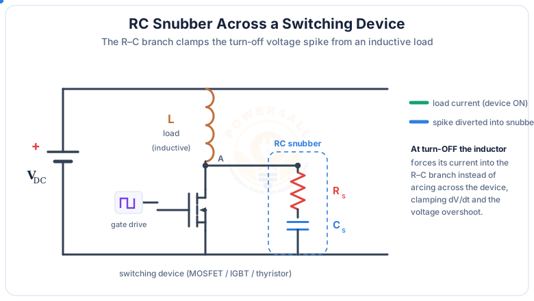
dV/dt and the voltage overshoot.The one-line idea
Inductance hates a sudden change of current, so it answers with a huge voltage. A snubber catches that energy in a capacitor and burns the resonance off in a resistor — a soft landing instead of a spike.
Why Snubbers Are Needed — The Switching Problem
The villain is inductance switching current. The defining law of an inductor is v = L (di/dt): interrupt the current quickly and di/dt is enormous, so the voltage is enormous too.
When a switch opens, the load and wiring inductance cannot stop conducting instantly. That current charges up the small stray capacitance across the device, overshooting far above the supply, and the leftover energy sloshes back and forth between the inductance and capacitance as ringing. Two bad things follow: the peak can exceed the device's breakdown rating, and the fast edges radiate electromagnetic interference.
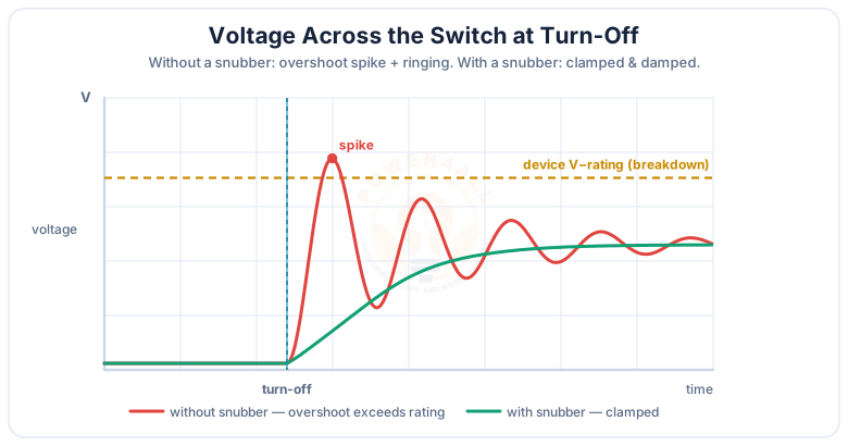
A fast turn-off (large di/dt) across even a small stray inductance produces a large voltage spike. The snubber caps the dV/dt and diverts the energy so this spike never reaches the device.
Real numbers
Switching 10 A off in 50 ns through just 100 nH of stray inductance gives v = 100n × (10/50n) = 20 V of overshoot per 100 nH — and real loops have several hundred nanohenries plus ringing gain. That is how a 400 V bus can spike a 600 V device to failure.
The RC Snubber
The workhorse snubber is the RC snubber: a capacitor in series with a resistor wired straight across the switch (or across the diode, or across the transformer winding).
The two parts share the work. The capacitor soaks up the turn-off energy and slows the voltage rise — a low dV/dt. The resistor damps the resonance between the circuit inductance and the capacitance so the waveform settles instead of ringing, and it limits the capacitor's discharge current when the switch turns back on. Get the resistor right and an underdamped ring becomes a clean, critically-damped edge.
The circuit rings at the resonance of the stray inductance L and capacitance C. The snubber capacitor lowers this frequency and the snubber resistor damps it. Matching the resistor to the loop impedance √(L/C) gives near-critical damping.
Worked example — damping a ring
A drain node rings at 20 MHz with an estimated loop inductance of 120 nH. The stray capacitance is C = 1/((2πf)²L) ≈ 0.53 nF. Choose a snubber capacitor a few times larger, Cs ≈ 1.5 nF, and a resistor near the new loop impedance Rs = √(L/Cs) = √(120n/1.5n) ≈ 9 Ω. That damps the ring without wasting excess power.
Types of Snubbers
There is a snubber for every job. The three you will meet most are the RC snubber, the RCD snubber, and the freewheeling-diode snubber.
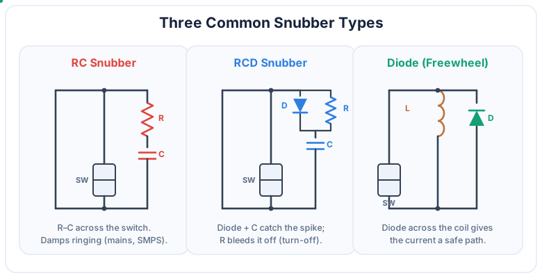
RC snubber
Simplest and most common; damps ringing across a switch, diode or transformer winding.
RCD (turn-off) snubber
Diode + capacitor catch the spike; a resistor bleeds the capacitor. Firmer clamp for IGBTs and thyristors.
Freewheeling diode
Across an inductive load; recirculates the coil current and clamps the voltage to one diode drop.
Turn-on (di/dt) snubber
A small series inductor slows the current rise at turn-on, cutting the turn-on loss.
Polarized vs non-polarized
Polarized snubbers (with a diode) act in one direction; plain RC snubbers act both ways.
Lossless / energy-recovery
Return the captured energy to the supply instead of burning it, for high-efficiency converters.
The RCD Clamp Snubber
In a flyback converter the transformer's leakage inductance stores energy that cannot cross to the secondary, and at turn-off it slams the switch drain with a spike. The classic cure is the RCD clamp snubber.
A diode lets the snubber capacitor charge fast the instant the drain rises, capturing the leakage energy; a parallel resistor then bleeds that capacitor down slowly between switching cycles. The diode's one-way action means the capacitor holds a firm clamp voltage instead of following the drain up and down — exactly what you want to pin a MOSFET or IGBT below its rating.
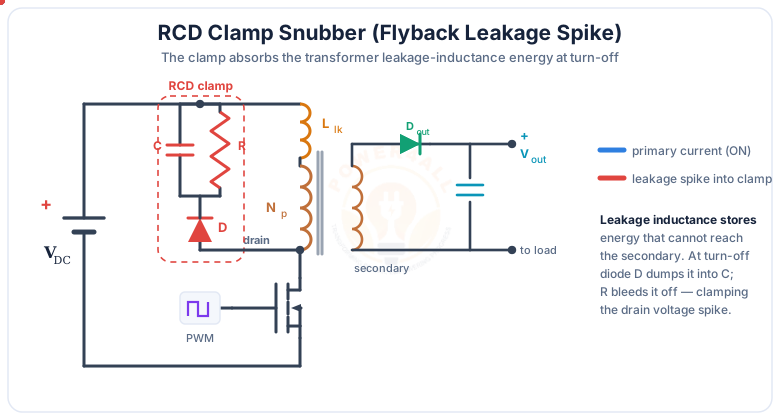
C through diode D at turn-off, and R bleeds it off — clamping the drain voltage spike.For a turn-off / dV/dt snubber, the capacitor is sized so the load current IL charging it cannot raise the voltage faster than the device (or an EMI target) allows: dV/dt = I/C, so a bigger capacitor means a gentler edge.
How to Design a Snubber
Snubber design is a balance: a bigger capacitor gives a softer edge but more loss, and the resistor must both damp the ring and survive the discharge. Here are the equations and the effect of the resistor value.
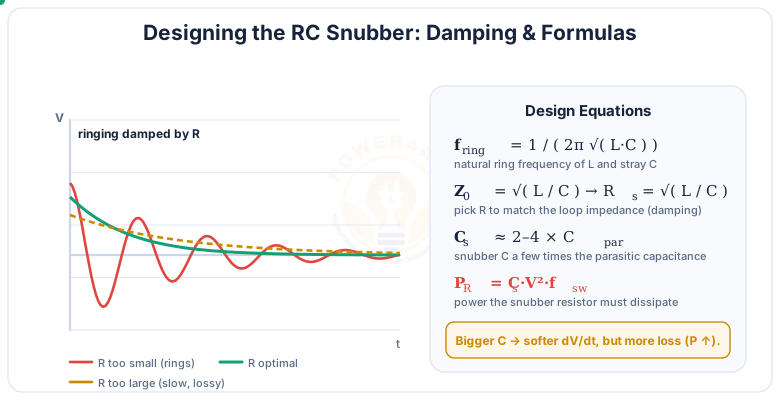
√(L/C) it lands cleanly. The card lists the working design equations.| Step | Equation | What it fixes |
|---|---|---|
| 1. Ring frequency | f = 1/(2π√(L·C)) | Find the stray L and C that are ringing. |
| 2. Snubber C | Cs ≈ 2–4 × Cpar or I/(dV/dt) | Absorb the energy / set the dV/dt. |
| 3. Snubber R | Rs = √(L/Cs) | Damp the resonance (near-critical). |
| 4. Discharge check | I = V/Rs, τ = RsCs « ton | Keep the turn-on current safe. |
| 5. Resistor power | PR = Cs·V²·fsw | Rate the resistor for the heat. |
Worked example — resistor power
A snubber uses Cs = 2.2 nF on a 400 V bus at fsw = 100 kHz. The resistor must dissipate PR = CsV²f = 2.2n × 400² × 100k ≈ 35 W… far too high — a clear signal to use a smaller capacitor, a lower clamp voltage (RCD), or a lossless snubber. Halving C or clamping at 200 V drops the loss dramatically.
Rule of thumb
Measure the actual ring frequency on a scope with and without a small known added capacitor to back out the real stray L and C. Then set Cs a few times the stray C and Rs = √(L/Cs), and finally check the resistor's power.
The Turn-Off Snubber & the Safe Operating Area
A turn-off snubber does more than protect against over-voltage — it reshapes the switching trajectory so high voltage and high current never occur together, keeping the device inside its Safe Operating Area (SOA).
During a hard turn-off the voltage rises while the current is still falling, so the device briefly sees both — a burst of V·I switching loss right at the SOA corner. A snubber capacitor holds the voltage low until the current has fallen, so the load line hugs the axes instead of bulging out.
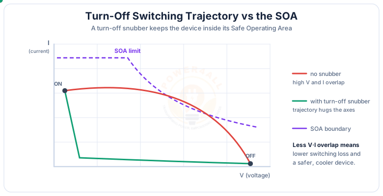
V and I overlap; with a snubber it hugs the axes and stays safely inside the SOA.Applications of Snubber Networks
Wherever a device switches inductive current, a snubber is close by — from a tiny DC–DC converter to a megawatt drive.
Inverters & H-bridges
Turn-off snubbers on IGBTs to control dV/dt and stay in the SOA.
Motor drives & VFDs
Snubbers cut dV/dt on inverter outputs, protecting windings and bearings.
Thyristor & triac circuits
RC snubbers prevent false dV/dt triggering of SCRs and triacs.
Relays & contactors
An RC snubber across the contacts suppresses arcing and extends contact life.
EMI reduction
Damping the ringing lowers conducted and radiated EMI, easing filter design.
Snubber vs Freewheeling Diode vs TVS / MOV
Three different components tame switching transients in three different ways. Here is when to reach for each.
| Snubber (RC / RCD) | Freewheeling diode | TVS diode / MOV | |
|---|---|---|---|
| Job | Damp dV/dt & ringing every cycle | Recirculate inductor current | Clamp occasional over-voltage / surge |
| Acts | Continuously, each switching edge | Whenever the switch opens | Only above its clamp threshold |
| Placed | Across the switch / diode / winding | Across the inductive load | Across the device or the bus |
| Energy | Burned in R (or recovered) | Circulated in the loop | Absorbed in the clamp |
They are complementary, not rivals: a well-designed converter may use a freewheeling diode for the load current, an RC/RCD snubber for the switching ring, and a TVS or MOV for surge protection — each covering what the others cannot.
Key Terms at a Glance
The essential snubber vocabulary engineers and students search for.
Snubber network
R–C(–D) circuit that tames switching transients.
dV/dt
Rate of rise of voltage the snubber limits.
RCD clamp
Diode-fed capacitor with a bleed resistor.
Leakage inductance
Uncoupled transformer L that causes the spike.
Ringing
Oscillation between stray L and C.
Safe Operating Area
V–I region the device may operate in.
Frequently Asked Questions
Quick, expert answers to the questions people ask most about snubber networks.
What is a snubber network?
A snubber network is a small circuit, usually a resistor and capacitor (RC) or a resistor, capacitor and diode (RCD), connected across a power switching device or an inductive load. It absorbs the energy stored in stray and leakage inductance at turn-off, limiting the voltage spike, the rate of rise of voltage (dV/dt) and the ringing that would otherwise stress or destroy the switch.
Why is a snubber needed?
When a switch interrupts current in an inductive circuit, the inductance opposes the sudden change and forces a large voltage spike (v = L di/dt) across the device, followed by ringing with stray capacitance. Without a snubber this overshoot can exceed the device breakdown voltage, cause EMI, and add switching loss. A snubber gives that energy a controlled path and clamps the voltage.
How does an RC snubber work?
An RC snubber places a capacitor in series with a resistor across the switch. The capacitor absorbs the turn-off energy and slows the rise of voltage, while the resistor damps the resonance between the circuit inductance and the capacitance so the waveform settles instead of ringing. The resistor also limits the capacitor discharge current when the switch turns back on.
What is an RCD snubber?
An RCD snubber adds a diode so the snubber capacitor charges quickly through the diode when the device turns off, capturing the spike, and then discharges slowly through the resistor between switching cycles. It is used as a turn-off snubber for IGBTs and thyristors and as a clamp across a flyback transformer to absorb the leakage-inductance energy.
What is the difference between an RC and an RCD snubber?
An RC snubber is symmetric: the capacitor charges and discharges through the same resistor every cycle, so it is simple but the resistor sees continuous loss. An RCD snubber separates the two paths with a diode, charging the capacitor fast through the diode and discharging it slowly through the resistor, which gives a firmer voltage clamp and is preferred for hard-switched IGBT, thyristor and flyback circuits.
How do I calculate the snubber capacitor?
For a dV/dt or turn-off snubber, size the capacitor from the load current and the allowed rate of voltage rise: Cs ≥ I / (dV/dt)max. For a damping RC snubber, choose Cs roughly two to four times the parasitic capacitance that is ringing, then set the resistor to damp the resonance.
How do I calculate the snubber resistor?
To damp the ringing, match the resistor to the characteristic impedance of the resonant loop: Rs ≈ √(L/C), where L is the stray or leakage inductance and C is the snubber capacitance. Also check that the resistor limits the capacitor discharge current at turn-on to a safe value (I = V/Rs) and that its RC time constant is short compared with the on-time.
How much power does a snubber resistor dissipate?
The snubber capacitor is charged and discharged every switching cycle, so the resistor dissipates about PR = Cs·V²·fsw, where V is the voltage the capacitor swings through. This is why a larger snubber capacitor gives a softer dV/dt but more loss, and why the resistor must be rated for that power.
What is the difference between a turn-on and a turn-off snubber?
A turn-off snubber is a capacitor (usually RCD) across the device that slows the voltage rise as it turns off, reducing the voltage-current overlap. A turn-on snubber is a small inductor in series with the device that slows the current rise as it turns on, reducing the current-voltage overlap. Both shrink the switching-loss area on the load line; hard-switched converters may use both.
Snubber vs freewheeling diode — what's the difference?
A freewheeling (flyback) diode is placed across an inductive load to give the inductor current a circulating path when the switch opens, clamping the voltage to about one diode drop. A snubber instead damps the fast dV/dt and high-frequency ringing across the switch itself. They solve related but different problems and are often used together.
Snubber vs TVS or MOV — which should I use?
A TVS diode or MOV is a voltage clamp that conducts only above a threshold and absorbs occasional large transients or surges. A snubber continuously shapes the switching waveform every cycle to control dV/dt and ringing. Use a snubber for repetitive switching stress and a TVS or MOV for surge and over-voltage protection; many designs use both.
Where are snubber networks used?
Snubbers are used across the switches of switch-mode power supplies, flyback and forward converters, buck and boost converters, inverters and H-bridges, motor drives and variable-frequency drives, thyristor and triac circuits, and across relay and contactor contacts to suppress arcing. Anywhere a device switches inductive current, a snubber controls the resulting spike and ringing.
Conclusion & Key Takeaways
A snubber network is the quiet guardian of every power switch: it catches the energy that inductance throws at the device, clamps the spike, damps the ring, and keeps the trajectory inside the safe operating area.
Tames the spike
Clamps turn-off over-voltage.
Damps ringing
R = √(L/C) for clean edges.
RC / RCD / diode
Pick the type for the job.
Design trade-off
Softer edge vs P = CV²f loss.
Stays in SOA
Reshapes the switching load line.
Everywhere
SMPS, inverters, drives, relays.